Download
1 / 29
290 likes | 437 Vues
Introduction to Field Programmable Gate Arrays. Lecture 1/3 CERN Accelerator School on Digital Signal Processing Sigtuna, Sweden, 31 May – 9 June 2007 Javier Serrano, CERN AB-CO-HT. Outline. Historical introduction. Basics of digital design. FPGA structure. Traditional (HDL) design flow.

E N D
Introduction to Field Programmable Gate Arrays Lecture 1/3 CERN Accelerator School on Digital Signal Processing Sigtuna, Sweden, 31 May – 9 June 2007 Javier Serrano, CERN AB-CO-HT
Outline • Historical introduction. • Basics of digital design. • FPGA structure. • Traditional (HDL) design flow. • Demo.
Outline • Historical introduction. • Basics of digital design. • FPGA structure. • Traditional (HDL) design flow. • Demo.
Historical Introduction • In the beginning, digital design was done with the ’74 series of chips. • Some people would design their own chips based on Gate Arrays, which were nothing else than an array of NAND gates:
Historical Introduction • The first programmable chips were PLAs (Programmable Logic Arrays): two level structures of AND and OR gates with user programmable connections. • Programmable Array Logic devices were an improvement in structure and cost over PLAs. Today such devices are generically called Programmable Logic Devices (PLDs).
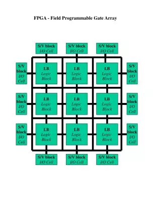
Historical introduction • A complex PLD (CPLD) is nothing else than a collection of multiple PLDs and an interconnection structure. • Compared to a CPLD, a Field Programmable Gate Array (FPGA) contains a much larger number of smaller individual blocks + large interconnection structure that dominates the entire chip.
Outline • Historical introduction. • Basics of digital design. • FPGA structure. • Traditional (HDL) design flow. • Demo.
Basics of digital design • Unless you really know what you are doing, stick to synchronous design: sandwiching bunches of combinational logic in between flip flops. • Combinational logic: state of outputs depend on current state of inputs alone (forgetting about propagation delays for the time being). E.g. AND, OR, mux, decoder, adder... • D-type Flip flops propagate D to Q upon a rising edge in the clk input. • Synchronous design simplifies design analysis, which is good given today’s logic densities.
Don’t do this! Toggle flip-flops get triggered by glitches produced by different path lengths of counter bits.
Basics of (synchronous) Digital Design High clock rate: 144.9 MHz on a Xilinx Spartan IIE. 6.90 ns Higher clock rate: 151.5 MHz on the same chip. 6.60 ns Illustrating the latency/throughput tradeoff
Outline • Historical introduction. • Basics of digital design. • FPGA structure. • Traditional (HDL) design flow. • Demo.
The logic block: a summary view Example: using a LUT as a full adder.
A practical example: Xilinx Virtex II Pro family (used in the lab) Configurable Logic Block (CLB) Overview Embedded PowerPC Digitally Controlled Impedance (DCI)
A practical example: Xilinx Virtex II Pro family Slice Detail of half-slice
A practical example: Xilinx Virtex II Pro family Routing resources
FPGA state of the art • In addition to logic gates and routing, in a modern FPGA you can find: • Embedded processors (soft or hard). • Multi-Gb/s transceivers with equalization and hard IP for serial standards as PCI Express and Gbit Ethernet. • Lots of embedded MAC units, with enough bits to implement single precision floating point arithmetic efficiently. • Lots of dual-port RAM. • Sophisticated clock management through DLLs and PLLs. • System monitoring infrastructure including ADCs. • On-substrate decoupling capacitors to ease PCB design. • Digitally Controlled Impedance to eliminate on-board termination resistors.
Why use embedded processors? Customization: take only the peripherals you need and replicate them as many times as needed. Create your own custom peripherals. Strike optimum balance in system partitioning.
Serial signaling • Avoids clock/data skew by using embedded clock. • Reduces EMI and power consumption. • Simplifies PCB routing.
Outline • Historical introduction. • Basics of digital design. • FPGA structure. • Traditional (HDL) design flow. • Demo.
Implement your design using VHDL or Verilog BehavioralSimulation HDL HDL Functional Simulation Synthesis TimingSimulation Implementation In-Circuit Verification Download Traditional design flow 1/3
BehavioralSimulation HDL HDL Synthesize the design to create an FPGA netlist Functional Simulation Synthesis TimingSimulation Implementation In-Circuit Verification Download Traditional design flow 2/3
BehavioralSimulation HDL HDL Functional Simulation Synthesis Translate, place and route, and generate a bitstream to download in the FPGA TimingSimulation Implementation In-Circuit Verification Download Traditional design flow 3/3
VHDL 101 Both VHDL code segments produce exactly the same hardware.
Outline • Historical introduction. • Basics of digital design. • FPGA structure. • Traditional (HDL) design flow. • Demo.
Demo • Now, let’s see how you go from design idea to hardware, using the traditional flow. • Many thanks to Jeff Weintraub (Xilinx University Program), Bob Stewart (University of Strathclyde) and Silica for some of the slides.