Download
1 / 41
410 likes | 417 Vues
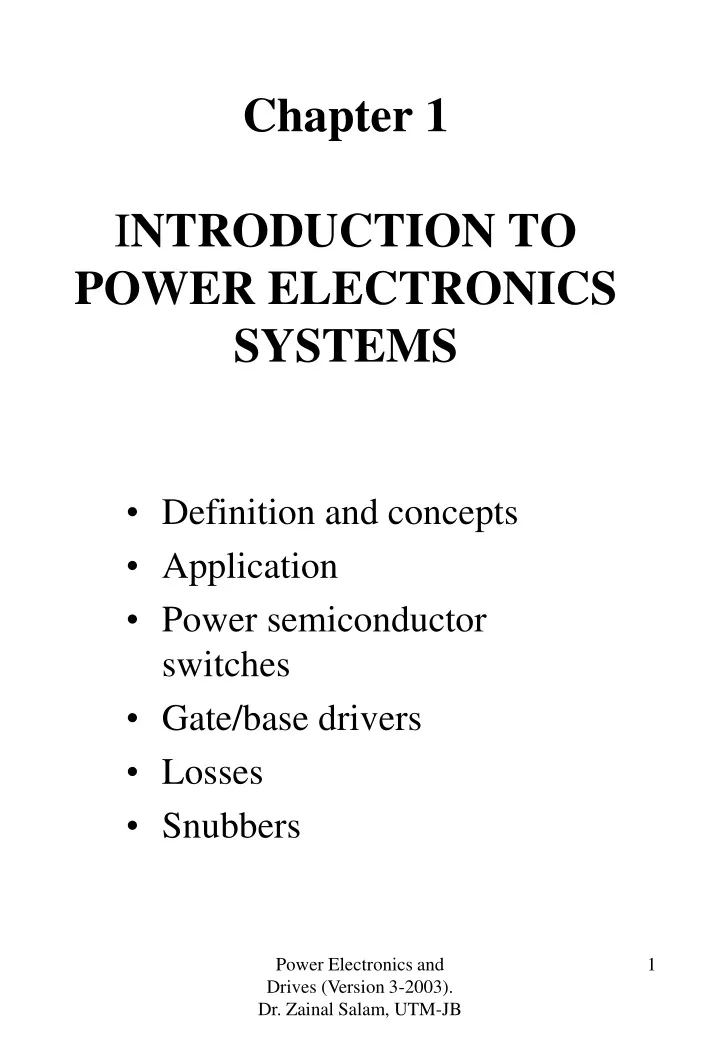
Chapter 1 I NTRODUCTION TO POWER ELECTRONICS SYSTEMS. Definition and concepts Application Power semiconductor switches Gate/base drivers Losses Snubbers. POWER INPUT. POWER OUTPUT. v i , i i. Power Processor. v o , i o. Source. Load. measurement. Controller. reference.

E N D
Chapter 1INTRODUCTION TO POWER ELECTRONICS SYSTEMS • Definition and concepts • Application • Power semiconductor switches • Gate/base drivers • Losses • Snubbers Power Electronics and Drives (Version 3-2003). Dr. Zainal Salam, UTM-JB
POWER INPUT POWER OUTPUT vi , ii Power Processor vo , io Source Load measurement Controller reference Definition of Power Electronics DEFINITION: To convert, i.e to process and control the flow of electric power by supplying voltage s and currents in a form that is optimally suited for user loads. • Basic block diagram • Building Blocks: • Input Power, Output Power • Power Processor • Controller Power Electronics and Drives (Version 3-2003). Dr. Zainal Salam, UTM-JB
Power Electronics (PE) Systems • To convert electrical energy from one form to another, i.e. from the source to load with: • highest efficiency, • highest availability • highest reliability • lowest cost, • smallest size • least weight. • Static applications • involves non-rotating or moving mechanical components. • Examples: • DC Power supply, Un-interruptible power supply, Power generation and transmission (HVDC), Electroplating, Welding, Heating, Cooling, Electronic ballast • Drive applications • intimately contains moving or rotating components such as motors. • Examples: • Electric trains, Electric vehicles, Air-conditioning System, Pumps, Compressor, Conveyer Belt (Factory automation). Power Electronics and Drives (Version 3-2003). Dr. Zainal Salam, UTM-JB
Application examples Static Application: DC Power Supply AC voltage DC-DC DIODE FILTER LOAD CONVERTER RECTIFIER AC LINE VOLTAGE V control F F (1 or 3 ) (derived from feedback circuit) Drive Application: Air-Conditioning System Power Electronics and Drives (Version 3-2003). Dr. Zainal Salam, UTM-JB
Vs (Volt) time + Vs _ Vo Vdc time Power Conversion concept: example • Supply from TNB: 50Hz, 240V RMS (340V peak). Customer need DC voltage for welding purpose, say. • TNB sine-wave supply gives zero DC component! • We can use simple half-wave rectifier. A fixed DC voltage is now obtained. This is a simple PE system. + Vo _ Power Electronics and Drives (Version 3-2003). Dr. Zainal Salam, UTM-JB
ig v ia s + vs _ + vo _ w w w t t t vo i g a Conversion Concept How if customer wants variable DC voltage? More complex circuit using SCR is required. By controlling the firing angle, a,the output DC voltage (after conversion) can be varied.. Obviously this needs a complicated electronic system to set the firing current pulses for the SCR. Power Electronics and Drives (Version 3-2003). Dr. Zainal Salam, UTM-JB
Power Electronics Converters DC input DC output AC input DC output DC input AC output AC to DC: RECTIFIER DC to DC: CHOPPER DC to AC: INVERTER Power Electronics and Drives (Version 3-2003). Dr. Zainal Salam, UTM-JB
Current issues 1. Energy scenario • Need to reduce dependence on fossil fuel • coal, natural gas, oil, and nuclear power resource Depletion of these sources is expected. • Tap renewable energy resources: • solar, wind, fuel-cell, ocean-wave • Energy saving by PE applications. Examples: • Variable speed compressor air-conditioning system: 30% savings compared to thermostat-controlled system. • Lighting using electronics ballast boost efficiency of fluorescent lamp by 20%. 2. Environment issues • Nuclear safety. • Nuclear plants remain radioactive for thousands of years. • Burning of fossil fuel • emits gases such as CO2, CO (oil burning), SO2, NOX (coal burning) etc. • Creates global warming (green house effect), acid rain and urban pollution from smokes. • Possible Solutions by application of PE. Examples: • Renewable energy resources. • Centralization of power stations to remote non-urban area. (mitigation). • Electric vehicles. Power Electronics and Drives (Version 3-2003). Dr. Zainal Salam, UTM-JB
PE growth • PE rapid growth due to: • Advances in power (semiconductor) switches • Advances in microelectronics (DSP, VLSI, microprocessor/microcontroller, ASIC) • New ideas in control algorithms • Demand for new applications • PE is an interdisciplinary field: • Digital/analogue electronics • Power and energy • Microelectronics • Control system • Computer, simulation and software • Solid-state physics and devices • Packaging • Heat transfer Power Electronics and Drives (Version 3-2003). Dr. Zainal Salam, UTM-JB
Power semiconductor devices (Power switches) • Power switches: work-horses of PE systems. • Operates in two states: • Fully on. i.e. switch closed. • Conducting state • Fully off , i.e. switch opened. • Blocking state • Power switch never operates in linear mode. • Can be categorised into three groups: • Uncontrolled: Diode : • Semi-controlled: Thyristor (SCR). • Fully controlled: Power transistors: e.g. BJT, MOSFET, IGBT, GTO, IGCT Power Electronics and Drives (Version 3-2003). Dr. Zainal Salam, UTM-JB
Photos of Power Switches (From Powerex Inc.) • Power Diodes • Stud type • “Hockey-puck” type • IGBT • Module type: Full bridge and three phase • IGCT • Integrated with its driver Power Electronics and Drives (Version 3-2003). Dr. Zainal Salam, UTM-JB
Id A (Anode) + Vd _ Id Vr Vf Vd K (Cathode) Diode: Symbol Power Diode v-i characteristics • When diode is forward biased, it conducts current with a small forward voltage (Vf) across it (0.2-3V) • When reversed (or blocking state), a negligibly small leakage current (uA to mA) flows until the reverse breakdown occurs. • Diode should not be operated at reverse voltage greater than Vr Power Electronics and Drives (Version 3-2003). Dr. Zainal Salam, UTM-JB
IF trr= ( t2 - t0 ) t2 t0 VR IRM VRM Reverse Recovery • When a diode is switched quickly from forward to reverse bias, it continues to conduct due to the minority carriers which remains in the p-n junction. • The minority carriers require finite time, i.e, trr (reverse recovery time) to recombine with opposite charge and neutralise. • Effects of reverse recovery are increase in switching losses, increase in voltage rating, over-voltage (spikes) in inductive loads Power Electronics and Drives (Version 3-2003). Dr. Zainal Salam, UTM-JB
Softness factor, Sr Snap-off IF Sr= ( t2 - t1 )/(t1 - t0) = 0.3 t0 VR t1 t2 Soft-recovery Sr= ( t2 - t1 )/(t1 - t0) = 0.8 IF t1 t2 t0 VR Power Electronics and Drives (Version 3-2003). Dr. Zainal Salam, UTM-JB
Types of Power Diodes • Line frequency (general purpose): • On state voltage: very low (below 1V) • Large trr(about 25us) (very slow response) • Very high current ratings (up to 5kA) • Very high voltage ratings(5kV) • Used in line-frequency (50/60Hz) applications such as rectifiers • Fast recovery • Very low trr (<1us). • Power levels at several hundred volts and several hundred amps • Normally used in high frequency circuits • Schottky • Very low forward voltage drop (typical 0.3V) • Limited blocking voltage (50-100V) • Used in low voltage, high current application such as switched mode power supplies. Power Electronics and Drives (Version 3-2003). Dr. Zainal Salam, UTM-JB
Ia A (Anode) Ia Ig>0 Ig=0 + Vak _ Ih Ig Vr Ibo G (Gate) Vak Vbo K (Cathode) Thyristor: Symbol Thyristor (SCR) v-i characteristics • If the forward breakover voltage (Vbo) is exceeded, the SCR “self-triggers” into the conducting state. • The presence of gate current will reduce Vbo. • “Normal” conditions for thyristors to turn on: • the device is in forward blocking state (i.e Vak is positive) • a positive gate current (Ig) is applied at the gate • Once conducting, the anode current is latched. Vak collapses to normal forward volt-drop, typically 1.5-3V. • In reverse -biased mode, the SCR behaves like a diode. Power Electronics and Drives (Version 3-2003). Dr. Zainal Salam, UTM-JB
ig v ia s + vs _ w w w t t t vo i g a Thyristor Conduction + vo _ • Thyristor cannot be turned off by applying negative gate current. It can only be turned off if Iagoes negative (reverse) • This happens when negative portion of the of sine-wave occurs (natural commutation), • Another method of turning off is known as “forced commutation”, • The anode current is “diverted” to another circuitry. Power Electronics and Drives (Version 3-2003). Dr. Zainal Salam, UTM-JB
Types of thyristors • Phase controlled • rectifying line frequency voltage and current for ac and dc motor drives • large voltage (up to 7kV) and current (up to 4kA) capability • low on-state voltage drop (1.5 to 3V) • Inverter grade • used in inverter and chopper • Quite fast. Can be turned-on using “force-commutation” method. • Light activated • Similar to phase controlled, but triggered by pulse of light. • Normally very high power ratings • TRIAC • Dual polarity thyristors Power Electronics and Drives (Version 3-2003). Dr. Zainal Salam, UTM-JB
Controllable switches (power transistors) • Can be turned “ON”and “OFF” by relatively very small control signals. • Operated in SATURATION and CUT-OFF modes only. • No “linear region” operation is allowed due to excessive power loss. • In general, power transistors do not operate in latched mode. • Traditional devices: Bipolar junction transistors (BJT), Metal oxide silicon field effect transistor ( MOSFET), Insulated gate bipolar transistors (IGBT), Gate turn-off thyristors (GTO) • Emerging (new) devices: Gate controlled thyristors (GCT). Power Electronics and Drives (Version 3-2003). Dr. Zainal Salam, UTM-JB
C (collector) IC B (base) + VCE _ IB IB E (emitter) VCE(sat) VCE v-i characteristics Bipolar Junction Transistor (BJT) IC BJT: symbol (npn) • Ratings: Voltage: VCE<1000, Current: IC<400A. Switching frequency up to 5kHz. Low on-state voltage: VCE(sat) : 2-3V • Low current gain (b<10). Need high base current to obtain reasonable IC . • Expensive and complex base drive circuit. Hence not popular in new products. Power Electronics and Drives (Version 3-2003). Dr. Zainal Salam, UTM-JB
C (collector) Driver Transistor IC1 IC Output Transistor B (base) IC2 + VCE _ IB1 IB2 Biasing/ stabilising network E (emitter) BJT Darlington pair • Normally used when higher current gain is required Power Electronics and Drives (Version 3-2003). Dr. Zainal Salam, UTM-JB
D (drain) ID G (gate) ID + VDS _ + VGS _ + VGS _ S (source) VDS Metal Oxide Silicon Field Effect Transistor (MOSFET) MOSFET: symbol (n-channel) v-i characteristics • Ratings: Voltage VDS<500V, current IDS<300A. Frequency f >100KHz. For some low power devices (few hundred watts) may go up to MHz range. • Turning on and off is very simple. • To turn on: VGS =+15V • To turn off: VGS =0 V and 0V to turn off. • Gate drive circuit is simple Power Electronics and Drives (Version 3-2003). Dr. Zainal Salam, UTM-JB
MOSFET characteristics • Basically low voltage device. High voltage device are available up to 600V but with limited current. Can be paralleled quite easily for higher current capability. • Internal (dynamic) resistance between drain and source during on state, RDS(ON), , limits the power handling capability of MOSFET. High losses especially for high voltage device due to RDS(ON) . • Dominant in high frequency application (>100kHz). Biggest application is in switched-mode power supplies. Power Electronics and Drives (Version 3-2003). Dr. Zainal Salam, UTM-JB
C (collector) IC VGE + VCE _ G (gate) + VGE _ VCE(sat) VCE E (emitter) v-i characteristics IGBT: symbol Insulated Gate Bipolar Transistor (IGBT) IC • Combination of BJT and MOSFET characteristics. • Gate behaviour similar to MOSFET - easy to turn on and off. • Low losses like BJT due to low on-state Collector-Emitter voltage (2-3V). • Ratings: Voltage: VCE<3.3kV, Current,: IC<1.2kA currently available. Latest: HVIGBT 4.5kV/1.2kA. • Switching frequency up to 100KHz. Typical applications: 20-50KHz. Power Electronics and Drives (Version 3-2003). Dr. Zainal Salam, UTM-JB
Ia A (Anode) Ia Ig>0 Ig=0 + Vak _ Ih Vr Ibo Ig Vak Vbo K (Cathode) GTO: Symbol Gate turn-off thyristor (GTO) G (Gate) v-i characteristics • Behave like normal thyristor, but can be turned off using gate signal • However turning off is difficult. Need very large reverse gate current (normally 1/5 of anode current). • Gate drive design is very difficult due to very large reverse gate current at turn off. • Ratings: Highest power ratings switch: Voltage: Vak<5kV; Current: Ia<5kA. Frequency<5KHz. • Very stiff competition: Low end-from IGBT. High end from IGCT Power Electronics and Drives (Version 3-2003). Dr. Zainal Salam, UTM-JB
Insulated Gate-Commutated Thyristor (IGCT) Ia + Vak _ IGCT Ig K (Cathode) A (Anode) IGCT: Symbol • Among the latest Power Switches. • Conducts like normal thyristor (latching), but can be turned off using gate signal, similar to IGBT turn off; 20V is sufficent. • Power switch is integrated with the gate-drive unit. • Ratings: • Voltage: Vak<6.5kV; Current: Ia<4kA. Frequency<1KHz. Currently 10kV device is being developed. • Very low on state voltage: 2.7V for 4kA device Power Electronics and Drives (Version 3-2003). Dr. Zainal Salam, UTM-JB
1GW Thyristor 10MW GTO/IGCT 10MW 1MW IGBT 100kW 10kW MOSFET 1kW 100W 10MHz 100kHz 1MHz 10Hz 1kHz Power Switches: Power Ratings Power Electronics and Drives (Version 3-2003). Dr. Zainal Salam, UTM-JB
(Base/gate) Driver circuit Driver Circuit Control Circuit Power switch • Interface between control (low power electronics) and (high power) switch. • Functions: • Amplification: amplifies control signal to a level required to drive power switch • Isolation: provides electrical isolation between power switch and logic level • Complexity of driver varies markedly among switches. • MOSFET/IGBT drivers are simple • GTO and BJT drivers are very complicated and expensive. Power Electronics and Drives (Version 3-2003). Dr. Zainal Salam, UTM-JB
+VGG From control circuit + VDC _ R1 Rg D G Q1 + VGS _ S LM311 Amplification: Example: MOSFET gate driver • Note: MOSFET requires VGS =+15V for turn on and 0V to turn off. LM311 is a simple amp with open collector output Q1. • When B1 is high, Q1 conducts. VGS is pulled to ground. MOSFET is off. • When B1 is low, Q1 will be off. VGS is pulled to VGG. If VGG is set to +15V, the MOSFET turns on. • Effectively, the power to turn-on the MOSFET comes form external power supply, VGG Power Electronics and Drives (Version 3-2003). Dr. Zainal Salam, UTM-JB
From control circuit D1 Q1 A1 To driver Isolation R1 ig + vak - Pulse source R2 iak Isolation using Pulse Transformer Isolation using Opto-coupler Power Electronics and Drives (Version 3-2003). Dr. Zainal Salam, UTM-JB
Switches comparisons (2003) Power Electronics and Drives (Version 3-2003). Dr. Zainal Salam, UTM-JB
Application examples • For each of the following application, choose the best power switches and reason out why. • An inverter for the light-rail train (LRT) locomotive operating from a DC supply of 750 V. The locomotive is rated at 150 kW. The induction motor is to run from standstill up to 200 Hz, with power switches frequencies up to 10KHz. • A switch-mode power supply (SMPS) for remote telecommunication equipment is to be developed. The input voltage is obtained from a photovoltaic array that produces a maximum output voltage of 100 V and a minimum current of 200 A. The switching frequency should be higher than 100kHz. • A HVDC transmission system transmitting power of 300 MW from one ac system to another ac system both operating at 50 Hz, and the DC link voltage operating at 2.0 kV. Power Electronics and Drives (Version 3-2003). Dr. Zainal Salam, UTM-JB
Power switch losses • Why it is important to consider losses of power switches? • to ensure that the system operates reliably under prescribed ambient conditions • so that heat removal mechanism (e.g. heat sink, radiators, coolant) can be specified. losses in switches affects the system efficiency • Heat sinks and other heat removal systems are costly and bulky. Can be substantial cost of the total system. • If a power switch is not cooled to its specified junction temperature, the full power capability of the switch cannot be realised. Derating of the power switch ratings may be necessary. • Main losses: • forward conduction losses, • blocking state losses • switching losses Power Electronics and Drives (Version 3-2003). Dr. Zainal Salam, UTM-JB
Heat Removal Mechanism SCR (stud-type) on air-cooled kits SCR (hokey-puck-type) on power pak kits Fin-type Heat Sink Assembly of power converters Power Electronics and Drives (Version 3-2003). Dr. Zainal Salam, UTM-JB
+Von- Ion Ion +Von- Real switch Ideal switch Forward conduction loss Ideal switch: • Zero voltage drop across it during turn-on (Von). • Although the forward current ( Ion ) may be large, the losses on the switch is zero. • Real switch: • Exhibits forward conduction voltage (on state) (between 1-3V, depending on type of switch) during turn on. • Losses is measured by product of volt-drop across the device Von with the current, Ion, averaged over the period. • Major loss at low frequency and DC Power Electronics and Drives (Version 3-2003). Dr. Zainal Salam, UTM-JB
Blocking state loss • During turn-off, the switch blocks large voltage. • Ideally no current should flow through the switch. But for real switch a small amount of leakage current may flow. This creates turn-off or blocking state losses • The leakage current during turn-off is normally very small, Hence the turn-off losses are usually neglected. Power Electronics and Drives (Version 3-2003). Dr. Zainal Salam, UTM-JB
P=vi i v v i Energy time time Real switching profile (turn-on) Ideal switching profile (turn on) Switching loss • Ideal switch: • During turn-on and turn off, ideal switch requires zero transition time. Voltage and current are switched instantaneously. • Power loss due to switching is zero • Real switch: • During switching transition, the voltage requires time to fall and the current requires time to rise. • The switching losses is the product of device voltage and current during transition. • Major loss at high frequency operation Power Electronics and Drives (Version 3-2003). Dr. Zainal Salam, UTM-JB
Vce +VL- Ls i Vce rated + Vce - + Vin - time Snubbers Simple switch at turn off • PCB construction, wire loops creates stray inductance, Ls. • Using KVL, Power Electronics and Drives (Version 3-2003). Dr. Zainal Salam, UTM-JB
Vce Ls + Vce - Vce rated time RCD Snubbers • The voltage across the switch is bigger than the supply (for a short moment). This is spike. • The spike may exceed the switch rated blocking voltage and causes damage due to over-voltage. • A snubber is put across the switch. An example of a snubber is an RCD circuit shown below. • Snubber circuit “smoothened” the transition and make the switch voltage rise more “slowly”. In effect it dampens the high voltage spike to a safe value. Power Electronics and Drives (Version 3-2003). Dr. Zainal Salam, UTM-JB
Snubbers • In general, snubbers are used for: • turn-on: to minimise large overcurrents through the device at turn-on • turn-off: to minimise large overvoltages across the device during turn-off. • Stress reduction: to shape the device switching waveform such that the voltage and current associated with the device are not high simultaneously. • Switches and diodes requires snubbers. However, new generation of IGBT, MOSFET and IGCT do not require it. Power Electronics and Drives (Version 3-2003). Dr. Zainal Salam, UTM-JB
Ideal vs. Practical power switch Power Electronics and Drives (Version 3-2003). Dr. Zainal Salam, UTM-JB