Download
1 / 1
10 likes | 73 Vues
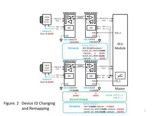
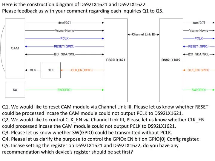
Here is the construction diagram of DS92LX1621 and DS92LX1622. Please feedback us with your comment regarding each inquiries Q1 to Q5.

E N D
Here is the construction diagram of DS92LX1621 and DS92LX1622. Please feedback us with your comment regarding each inquiries Q1 to Q5. Q1. We would like to reset CAM module via Channel Link III, Please let us know whether RESET could be processed incase the CAM module could not output PCLK to DS92LX1621. Q2. We would like to control CLK_EN via Channel Link III, Please let us know whether CLK_EN could processed incase the CAM module could not output PCLK to DS92LX1621. Q3. Please let us know whether SW(GPIO) could be transmitted without PCLK. Q4. Please let us clarify the purpose to control the GPIOx EN bit on GPIO[0] Config register. Q5. Incase setting the register on DS92LX1621 and DS92LX1622, do you have any recommendation which device’s register should be set first?