Download
1 / 16
160 likes | 350 Vues
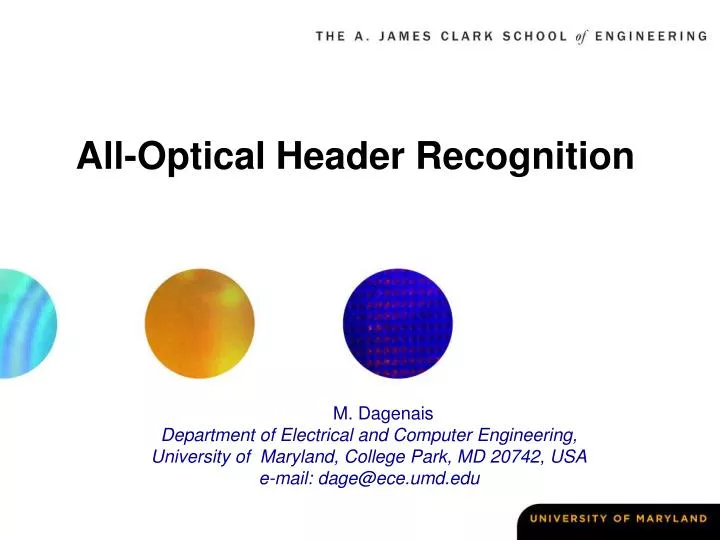
All-Optical Header Recognition. M. Dagenais Department of Electrical and Computer Engineering, University of Maryland, College Park, MD 20742, USA e-mail: dage@ece.umd.edu. Outline. Introduction Description of on-going work on optical header recognition Challenges and Opportunities

E N D
All-Optical Header Recognition M. Dagenais Department of Electrical and Computer Engineering, University of Maryland, College Park, MD 20742, USA e-mail: dage@ece.umd.edu
Outline • Introduction • Description of on-going work on optical header recognition • Challenges and Opportunities • Conclusion
Functionality of a Packet Switch • Routing • Reading destination address in packet header • Comparing destination address with local look-up table addresses • Setting up switch for payload switching • Flow Control and Contention Resolution • Accurate Synchronization between different modules within the switch • Header Regeneration/Reinsertion
Our Ultimate Goals for Optical Packet/Header Recognition • Technology scalable from 10 Gb/s to 160 Gb/s • 32 bit headers • Packets switchable on 1 ns time scale • Look-up table at network nodes containing up to 65,000 (2 bytes) addresses • Reprogrammable nodes
Present Goals of the Project • All-optical header recognition up to 160 Gb/s • 3 out of a 8-bit headers are used for destination address • Use successively one bit of header for steering packet in 1 x 2 space switches located at each level of a tree structure • Demonstrate header recognition (payload already pre-separated)
Research Goals • Implement packet routing in a network • Propose and demonstrate robust all- optical header recognition • Demonstrate a tree-based packet switched network operating up to 160Gb/s
Tree Structure for Header Recognition: Optical Packet Switch Slot 1 (clock bit) Output Slot 8 (clock bit) Address Slot 1 Y - space - Slot 8 switch es : 1…0000 process 2nd address bit Decision is made at each stage by taking the autocorrelation of header with a properly delayed copy of itself and thresholding the result Y - space - switch : 1…0001 st process 1 address bit 1…0010 1…0011 1…001 Input 1…0100 1…0101 Y - space - switch es : process 3rd address bit 1…0110 1…0111
Control Signals I1 SOA SOA I2 Non-Interferometric 1 x 2 Space Switch
Copy of header Optical Header Recognition Reading the fifth header bit Address Bits Control Bits Copy of header delayed by 4 bits
Output of the optical AND gate when the 5th bit is 1 for 10Gb/s data rate
Required Properties • Must provide considerable speed advantage and ability to simplify the circuit design • Switching energies should be similar to those of electronics or potentially less • Should have capability for integration • Should be scalable with the system bit rate and with transmission protocol • Should be polarization independent • Can be cascaded in several stages
Differential Mach-Zehnder Gate • Numerical models show potential for >500 GB/s • Achieved up to 336 Gb/s w/ integrated device • Achieved ~200 fs switching time at 10 GHz Rep. Rate • < 200 fJ switching energy • Requires two SOA’s • Not limited by carrier lifetime due to dual control pulses (differential mode) but limited by control pulse resolution
Guard time Header 2 Payload 2 Payload 1 10 ns 100 ns 2 ns Packet Schematic Full header recognition using a single AND gate: time domain
Full header recognition using a single AND gate: wavelength domain Programmable switch Mach-Zehnder Gate SOA
Challenges and Opportunities: Node Requirements for 32-bit Header Recognition at 160 Gb/s • Optical delay chips: • Required delays: 6ps X 32 = 192 ps 6 cm Solution: low loss passive waveguides on a chip: silica-on-silicon • Optical AND gate • Solution: Differential Mach-Zehnder gate switch • Serial-to-parallel converter • Time domain: combination of time delays, optical AND gate, and fast electronics • Wavelength domain: combination of time delays, arrayed-waveguide-gratings (AWG), SOAs, super-continuum fiber, and optical AND gate. • Tree network: optical packet switch • Integrated chip composed of “passive” (no gain) switches and active switches (with gain) Solution: Electro-absorption switches in a tree-structure integrated with SOAs to compensate for losses • Switch Programmability • Need to combine different packet switch output outcomes into several outputs in a programmable way • Packaging requirements • Hybrid integration required: delay chip based on silica-on-silicon; optical AND gate and amplification based on InP and electronics based on CMOS Solution: Silica-on-silicon optical bench
Conclusion • Application of ultrafast TDM technologies to photonic packet switching and optical header recognition was presented • Photonic header processing has the potential of being scaled up and even beyond 500 Gb/s (1.5 Tb/s demultiplexing already demonstrated). • The differential Mach-Zehnder gate is the most promising technology for implementing logic functions, given that it is ultra-fast (500 Gb/s possible) and requires low switching energy (< 200 fJ), • The use of a tree architecture allows flexibility. In particular, it can read all the possible headers. In addition, it allows the switch to be programmable.