Download
1 / 11
110 likes | 243 Vues
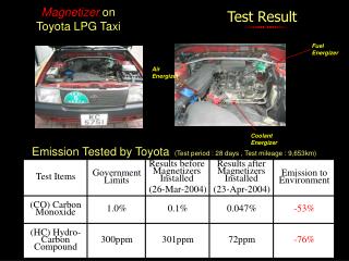
HBD FEE test result summary + production schedule. 16mv test pulse result 5X attenuator + 20:1 resistor divider at input (to reduce the noise on the test pulse input) Result on the digitized baseline noise Large input pulse Digital filter

E N D
HBD FEE test result summary+ production schedule • 16mv test pulse result • 5X attenuator + 20:1 resistor divider at input • (to reduce the noise on the test pulse input) • Result on the digitized baseline noise • Large input pulse • Digital filter • A nice, necessary, feature to remove the low frequency noise. • First look of the production schedule
FEE testing block diagram 20:1 attenuator FEM Pulse Generator Preamp Test Jig 5x attenuator ADC+FPGA receiver scope Pulse Generator trigger data Clock Master L1 trigger computer ADC Test point for receiver output Receiver
HBD ADC board FPGA ADC Receiver/ shaping Signals from Preamp
Test stand ADC module Preamp test jig
16MV test pulse on all the channels on FEM number 2 The test is done by moving test jigs cables (6 outputs) 8 times. 60Mhz noise kicks back from ADC Preamp output Output of FEM receiver 10mv, 100ns per division Digital sum 20mv/division
Digitized 16mv test pulse result 2 samples at rising edge 1-2 ns time jitter on the test pulse Reverse the signal cable RMS
RMS on the baseline in varies conditions 16mv test pulse generated about 210 ADC counts
Overflow pulse Preamp pulse 200mv, 20ns per division
Preamp pulse seen by channel 4 with noisy power line (100 events) A D C Digitized result samples Baseline distribution Sample # 4 ADC
Digital filtered preamp pulse on channel 4 data with noisy power line (100 events) pulse(n+2) –pulse(n) sample Baseline distribution Sample # 4 ADC
First look at production • Assume RUN 7 electronics installation in Sept 06. • One month contingency August • 2 months PCB production + assembly • We only have to build 50 FEMs. This time could be shorten. • Schedule final design review on the electronics. • chain test with detector • To understand ground, gain/shaping time of the FEM etc • Once the parts is solder to the PCB, it is final… • 3 months parts procurements • 1 month to generate P.O. and 2 months to get the parts • March is the time to buy parts. • Once we send out RFQ, we will know how good is the 3 months estimate. • Risks • March is the time to get ready for the RUN 6 test • Split manpower and attention