Download
1 / 10
100 likes | 275 Vues
Design and Automation Tool for STT-RAM. Anurag Nigam ECE-6502. Tasks Break-up . Leaf Cell Design a) Bit-cell b) Sense amplifier c) Timing block, Write Driver Testing 4x4 Memory Array Automated skill script to Generate the schematic Testing the complete memory array.

E N D
Design and Automation Tool for STT-RAM Anurag Nigam ECE-6502
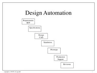
Tasks Break-up • Leaf Cell Design a) Bit-cell b) Sense amplifier c) Timing block, Write Driver • Testing 4x4 Memory Array • Automated skill script to Generate the schematic • Testing the complete memory array
Hard Ferro magnetic layer Oxide layer RP Free Ferro magnetic layer RAP STT-RAM bit cell overview • 1 Magnetic Tunnel Junction (MTJ) • 1 access transistor IMTJ = f(Vin, parameters) Fig1: Structure of MTJ
componentName = isource I = f(V) Bit-Cell Design: • Editing CDF parameter to create Behavioral Source • Parameterized bit-cell
WL BL=0V SL=1V Switching Write “1” Operation Bit-Cell Design Schematic
Sense Amplifier Design Reference: S. Natarajan et.al “ Searching for the Dream Embedded Memory”, ISSC Magazine 2009.
Write Driver: • Write “1” BL =0 SL=1 • Write “0” BL=1 SL=0 STT-RAM array automation: • Modified satya’s skill script to use leaf cells designed for STT-RAM. • 3 scripts for array, write driver and sense-amp. generation. • 1script to generate the complete schematic.
8x8 Array Write Driver Sense Amplifier Timing Block 8 x 8 Memory Array
Read “1” Write “0” Read “0” Write “1” clk data<0> out<0> 8x8 Memory Array: Results
Work in Progress ….. • Testing 8Kb memory block. • Delay-power optimization