Download
1 / 13
130 likes | 299 Vues
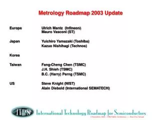
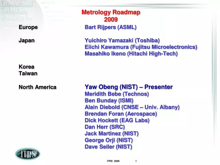
Metrology Roadmap 2009. Europe Bart Rijpers (ASML) Japan Yuichiro Yamazaki (Toshiba) Eiichi Kawamura (Fujitsu Microelectronics) Masahiko Ikeno (Hitachi High-Tech) Korea Taiwan North America Yaw Obeng (NIST) – Presenter Meridith Bebe ( Technos )

E N D
Metrology Roadmap2009 Europe Bart Rijpers (ASML) Japan Yuichiro Yamazaki (Toshiba) Eiichi Kawamura (Fujitsu Microelectronics) Masahiko Ikeno (Hitachi High-Tech) Korea Taiwan North AmericaYaw Obeng (NIST) – Presenter MeridithBebe (Technos) Ben Bunday (ISMI) Alain Diebold (CNSE – Univ. Albany) Brendan Foran (Aerospace) Dick Hockett (EAG Labs) Dan Herr (SRC) Jack Martinez (NIST) George Orji (NIST) Dave Seiler (NIST)
Lithography Metrology for Advanced Patterning Spacer Patterning Double Exposure Double Patterning 2p CD p/2 Spacers Metrology Need: Latent Image CD CD-AFM after both exposures but no Solution for CD between exposures Metrology Need: Overlay with Precision of 70% Of Single Layer Metrology Need: Spacer Thickness on Sidewall Spacer Profile 22 nm Dense lines
Metrology Challenges for Advanced Litho Processes 2 Population CD, SWA, height and pitch Potential Solution -> scatterometry Q: is there enough sensitivity for odd-even line scenario Metrology for Latent Image at 1st exposure might be avoided using AEC/APC approaches & CD/Overlay after double exposure
Contour Metrology • For CD-SEMs, Design-Based Metrology (DBM) applications allow for practical SEM verification of design intent, through the collection of feature 2D contour shape information and comparison to GDS files. • automatic CD-SEM recipe setup from design information • DBM applications very important for development and verification of OPC • number of measurements for successfully developing OPC is expected to grow exponentially with technology generation. • metrology interfaces with the Design for Manufacturing (DFM) community. • Contour fidelity is a prevailing challenge • Accuracy of contour extraction strong implications for OPC • Accuracy of registration strong implications for in-die overlay • Remaining work : define: • contour error source testing methodologies • contour reference metrology • SEM modeling for contours
FEP Metrology Gaps • SOI • Thickness down to 2nm • Defects in SOI layer • General • 450mm wafers • 1.5mm EE • Wafer Flatness • Particles Detection • size, composition • New High K – Metal Gate Materials • 3-D Profiling of Gates, Channel and S-D • III-V and SiGe Channels • Defects • Lattice Misfits • Interfaces • New Memory Materials • Phase Change Memory – polycrystalline chalcogenide) • Spintronic / Magnetic Films • CIPT needed
FEP Metrology • 3D Metrology – Complex structure measurement and • inspection are required • e.g. high A/R holes, film thickness & properties on sidewall Pipe-shaped BiCS Flash Memory (R. Katsumata, Toshiba) TCAT (Terabit Cell Array Transistor) (J. Jang, Samsung)
Measurement Point Local Strain/Stress Measurement Relatively small laser spot (Visible light) with deeper penetration pMOS nMOS Ghani, et al (Intel) Stress Liner Wide laser spot for extracting average stress STI STI Channel Strain/Stress Small laser spot for extracting single Tr. stress Cross sectioning for TEM
Local Stress/Strain Measurement Method Sensitivity Measurement Method Measurement Area Sample Thickness Area of Interest Stress Strain Transistor Level - SEM EBSD Destructive - CBED - NBD - TERS 20 MPa 100 MPa 50 MPa 0.02% 0.1% 0.05% 10-20nm ~10nm <50nm <100nm <300nm Destructive Destructive Destructive Micro-Area Level 20MPa 10 MPa <20MPa 0.02% 0.01% <0.02% ~150nm 100um 1um - Confocal Raman - XRD - Photo reflectance Spectroscopy Non-Destructive Non-Destructive Die - Die level flatness - Laser Interferometry - Coherent Gradient Sensing Non-Destructive Wafer - Laser Interferometry - Coherent Gradient Sensing Non-Destructive TERS (Tip Enhanced Raman Scattering) CBED (Convergent Beam Electron Diffraction) NBD (Nano Beam Electron Diffraction) XRD (X-ray Diffraction) * Stress – Strain relation : need to be clarified
2009 Interconnect Metrology • Existing Challenges • Measurement Gap - Sidewall barrier thickness and sidewall damage (compositional changes in low k) • New - Porous low k is projected for 22 nm ½ Pitch • Detection of Voids after electroplating • Monolayer interface for new barrier-low k • Air Gap sacrificial layer does not require unique metrology • Metrology is needed for 3D Integration • TSV Depth and Profile through multiple layers • Alignment of chips for stacking – wafer level integration • Bond strength • Defects in bonding • Damage to metal layers • Defects in vias between wafers • Through Si via is high aspect ratio CD issue • Wafer thickness and TTV after thinning • Defects after thinning including wafer edge • Emerging / Gated Interconnects • Native Deice Interconnects
Metrology for ERM/ERD High carrier mobility and structural robustness have driven a considerable effort in Graphene research Measurement of Bi-layer misorientation Aberration corrected TEM How many Layers? Raman and LEEM Quantum Hall Effect observes the Berry Phase
Metrology Summary 3D Metrology for Advanced Memory • FEP-Interconnect-Litho • PC and SST RAM - New materials for Metrology • Dual Patterning • 3D Metrology – Confirm Geometry Requirements e.g. film thickness & properties on sidewall • Reference Methods for 3D • Composition & Stress – e.g. buried channels • EUV metrology requirements • ERD-ERM • Standardization of Measurements • Properties of low Dimensional Materials • Microscopy and feature size/function • Time resolved magnetic measurements • Dimensional and Temporal Resolution of Local Structures and Dynamics • Ability to perform real time measurements, e.g. phase transitions, transport properties, memory switching times, domain dynamics Graphene – C. Kisielowski