Download
1 / 26
260 likes | 461 Vues
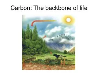
Serguei Brazovskii and Natasha Kirova Natal 2012 Physics of synthetic conductors as low dimensional correlated electronic systems. Lecture 1, part 2. THE WOLD OF CARBON. Energy. Crystal. Isolated atom. « More is different . » P.W. Anderson. Molecular crystals ,

E N D
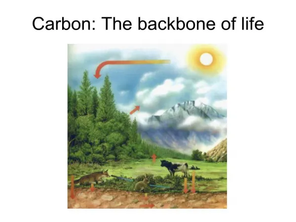
SergueiBrazovskii and Natasha Kirova Natal 2012 Physics of synthetic conductors as low dimensional correlated electronic systems. Lecture 1, part 2 THE WOLD OF CARBON
Energy Crystal Isolated atom « More isdifferent. »P.W. Anderson Molecularcrystals, narrow bands, propertiesare determinedmainly by individualmolecules Metals, semiconductors, dielectrics, band picture
All Dimesionalities from Carbon • 0D quantum dots – C60 • 1D quantum wires – carbon nanotubes • 1D polymer chain – carbyne -(C C)- • 2D layer - graphene • 2D layered material - graphite • 3D wide gap semicond. - diamond
Zero dimensional: • Fullerene (C60) –socker ball • Cage diameter - 0.71 nm • Optical gap – 1.9 V • Crystalline Fullerene • fcc structure • with lattice constant of 1.417 nm • C60-C60 distance – 1.002 nm
Multi-wall 1991 Single-wall 1993 1nm AFM image One dimensional: Carbon nanotubes Carbyne – linear polymer chain of C atoms Yung modulus 40 times of diamond Can be very good conductor thin (1nm) and resistant
Two dimensional - graphene Basic block – benzene ring
Three dimensional: graphite; diamond
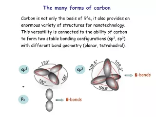
Q. Where the difference comes from? A. Hybridization of the orbitals. Q. Why we need the hybridization? A. We gain the kinetic energy. Q. What does it mean the hybridization? A. See next slides.
Carbon Atomic Orbitals • Carbon has 6 electrons. • Average atomic weight 12.011 amu • Electronic configuration: 1s22s22p2 2p2 2s2 1s2
p and s bonds • Two side-to-side 2porbitals form a p bond. • Two co-axial 2porbitalsform the s bond.
Carbon: Hybridized Orbitals There are four valence electrons. In the ground state valence is 2 (rem. CO). But electron can easy come from 2s2 to 2p2, now the valence is 4 (rem. CO2). 2p2 2s2 1s2 The 2s and 2p wave functions can mix forming hybridized orbitals.
Three possible types of mixing I. SP hybridization Carbyne – linear polymer
Graphite II. SP2 hybridization SP2
Diamond III. SP3 hybridization
Other carbon based materials Saturatedpolymers – traditional plastics SP3 Polyethylene (CH2)x – saturatedpolymerwith all saturated - bonds, all electronsform the chainsceleton H H H H H H C C C C C C H H H H H H SP2 Conjugatedpolymers: linearchains and phenylbasedones Polyacethylene (CH)x H H H H H H C C C C C C C C C C C C H H H H H H shouldbe a metalbut a dielectric, the energy gap 1.5eV
Conductivity of Organic Materials
Optically active polymers Main basic block benzene ring or modified benzene ring, hence SP2 hybridization
Carbon – carbon doping Fullerene in a blend with polymer –charge harvesting for photo-voltaic cells By light we excite electron-hole pair on the polymer chain and electron comes Very fast (10-13s) to the fullerene, so the electron is transfered from carbons of the polymer to the carbons of the fullerene
Some applications of the conducting polymers:Organicdevices Devices produced by UNIAX, the company of A. Heeger Chip made by Phillips Research Lab.
Organic displays OLED based TV
1D CRYSTALS Main ingredients Periodic lattice. In 1D: x→x+a Periodic reciprocal space k. In 1D k →k+G G=2π/a - π/a<k< π/a Quasi-momentap=ћk Energy spectra: for electrons E(k) for molecular vibrations (phonons) ћω(k)
E E Semiconductors: gap between HOMO and LUMO continuum p p Indirect gap Direct gap
Metals or heavily doped semiconductors E E p EF EF Semimetal, Ne=Nh(Bi, Sb, graphite, TTF-TCNQ) -pF pF EF p p -pF pF Zero point metal (graphene, some nanotubes) Hole metal Electron metal Overall shape for small number of particles: E δE=±vFδp m* - effective mass ( <1 for simple metals) Dimensionless parameter of e-e interaction
Bound states – semiconducting regime. Attractive point impurity, arbitrary dimension d=1, 2, 3. V(r)=-V0adδ(r) Assumption: the bound state localization length l>>a l -V0 a Wave function: Minimization over l: Energy: optimal y , i.e. optimal l d=1 E d=1 either collapse l→0 or unbinding l→∞ d=2 1/l d=3 E=Ay2-By3stable unbound state y=0, l=∞ d=3
Q. Band structure from small to infinite chains ? A. Lecture 2