Download
1 / 20
420 likes | 940 Vues
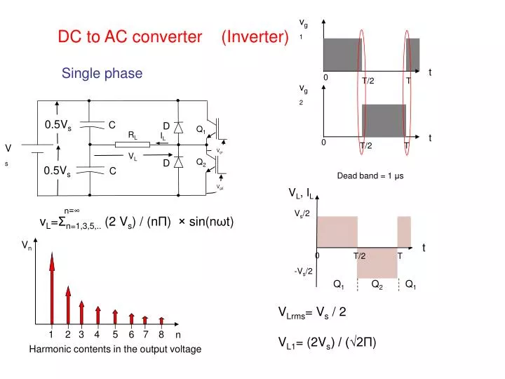
0. T/2. T. 0.5V s. C. D. Q 1. R L. I L. t. V s. V g 1. V L. Q 2. D. 0.5V s. C. Dead band = 1 μ s. 0. T/2. T. V g2. v g1. DC to AC converter (Inverter). Single phase. t. v g2. V L , I L. n=∞ v L = Σ n=1,3,5,.. (2 V s ) / (n Π ) × sin(n ω t). V s /2. V n. t. 0.

E N D
0 T/2 T 0.5Vs C D Q1 RL IL t Vs Vg1 VL Q2 D 0.5Vs C Dead band = 1 μs 0 T/2 T Vg2 vg1 DC to AC converter (Inverter) Single phase t vg2 VL, IL n=∞ vL=Σn=1,3,5,.. (2 Vs) / (nΠ) × sin(nωt) Vs/2 Vn t 0 T/2 T -Vs/2 Q1 Q2 Q1 VLrms= Vs / 2 VL1= (2Vs) / (√2Π) 1 2 3 4 5 6 7 8 n Harmonic contents in the output voltage
vL Vs/2 0.5Vs C D1 Q1 LL RL IL t 0 T/2 T Vs Vg1 VL Q2 D2 -Vs/2 0.5Vs C Q1 Q2 Q1 Vg2 iL t D1 Q1 D2 Q2 Heavily inductive load (RL → 0) R-L load iL= Σ (2Vs) / [ nΠ√ (R2+n2ω2L2) ] × sin (nωt - Θn) Θn= tan-1(nωL / R)
Performance Parameters HFn Harmonic Factor for the nth harmonic HFn= (VLn) / VL1 for n > 1 THD Total Harmonic Distortion The harmonic voltage Vh ∞ THD = 1 / VL1 ( Σ V2n ) 0.5 n=2, 3, 4,… ∞ Vh= ( Σ VLn2 ) 0.5 = ( VLrms2 – VL12 )0.5 n= 3, 5, 7, .. DF Distortion Factor ∞5 DF = 1 / VL1 [ Σ ( VLn / n2 )2 ] 0.5 n=2, 3, … The Distortion Factor of the nth harmonic = VLn / ( VL1 n2) for n > 1 Lowest Order Harmonic LOH is the harmonic component that is the closest to the fundamental and its amplitude Is ≥ 3% of the fundamental
Calculate: a) The rms value of the load fundamental voltage. b) The output power. c) The average and peak current in the transistor. d) The THD, DF, the HF and DF of the LOH. 0.5Vs C D1 Q1 LL RL IL Vs Vg1 VL • a) vL1 = (2Vs) / Π × sin ( ωt) • VL1rms = ( 2 × 48 ) / ( Π × √2 ) = 21.6 V • VLrms= 0.5 Vs = 24 V • PL= (VLrms)2 / R = 242 / 2.4 = 240 W • c) Q2 D2 0.5Vs C Vs= 48V R= 2.4 Ω Vg2 iQ1 iQ2 t t 0 T/2 T 0 T T/2 Peak current in each transistor = 24/2.4 = 10A Average current in each transistor = 5 A DF = 1/21.6 ×{ [ 7.2/32]2+ [4.32/52]2 +[3.086/72] 2}0.5 = 1/21.6 ×{ 0.64 + 0.02986 +0.004+ .. }0.5 = 0.038 VL3= 21.6/3 = 7.2 V VL5= 21.6/5 = 4.32 V VL7= 21.6/7 = 3.086 V d) Vh= ( 242 – 21.62 )0.5 = 10.46 V THD = 10.46 / 21.6 = 0.4843
The LOH = 3rd harmonic HF3= 1/3 = 0.3333 DF3= 0.3333/32 = 0.03703 note that VL3= 0.3333 which is > 0.03 so LOH =3
0 T/2 T D D Q1 Q3 RL IL Vs Vg1 Vg3 VL Q2 D Q4 D t Vg4 Vg2 Dead band = 1 μs 0 T/2 T Vg1, Vg2 The H-bridge single phase inverter t Vg3, Vg4 VL, IL n=∞ vL=Σn=1,3,5,.. (4 Vs) / (nΠ) × sin(nωt) Vs Vn t 0 T/2 T -Vs Q1, Q2 Q1, Q2 Q3, Q4 VLrms= Vs VL1= (4Vs) / (√2Π) 1 2 3 4 5 6 7 8 n Harmonic contents in the output voltage
D D Q1 Q3 RL IL Vs Vg1 Vg3 VL Q2 D Q4 D Vg4 Vg2 Calculate: a) The rms value of the load fundamental voltage. b) The output power. c) The average and peak current in the transistor. d) The THD, DF, the HF and DF of the LOH. • a) vL1 = (4Vs) / Π × sin ( ωt) • VL1rms = ( 4 × 48 ) / ( Π × √2 ) = 43.2 V • VLrms= Vs = 48 V • PL= (VLrms)2 / R = 482 / 2.4 = 960 W • c) Vs= 48V R= 2.4 Ω iQ1, iQ2 iQ3, iQ4 t t 0 T/2 T 0 T T/2 Peak current in each transistor = 48/2.4 = 20A Average current in each transistor =10 A DF = 1/43.2 ×{ [ 14.4/32]2+ [8.64/52]2 +[6.17/72] 2}0.5 = 1/43.2 ×{ 1.6 + .3456 +0.1259+ .. }0.5 = 0.033 (same) VL3= 43.2/3 = 14.4 V VL5= 43.2/5 = 8.64 V VL7= 43.2/7 = 6.17 V d) Vh= (482 – 43.22 )0.5 = 20.92 V THD = 20.92 / 43.2 = 0.4843 (same)
LOH = 3rd harmonic HF3 = 1/3 DF3= 1/(3×32) = 0.03703 (same) note that VL3= 14.4 which is > 0.03×VL1 so LOH =3 The quality of the output voltage is the same as for the 2-transistor circuit however, the H bridge inverter the output power is 4 times higher and the fundamental output Voltage is twice that of the 2-transistor circuit.
D D Q1 Q3 C L R IL Vs Vg1 Vg3 VL Q2 D Q4 D Vg4 Vg2 • The H-bridge inverter shown in figure has an • RLC load with R=10Ω, L=31.5mH, C=112μF. • The inverter frequency is 60 Hz and the dc input • Voltage is Vs=220V. • Express the instantaneous load current in • Fourrier series. • Calculate the rms load current at the fundamental • frequency. • c) Calculate the THD of the load current. • d) Calculate the total power absorbed by the load as well as the fundamental power. • e) Calculate the average dc current drawn from the supply. • f) Calculate the rms and the peak current of each transistor.
D3 D5 D1 Q1 Q5 Q3 R c b a a Vg5 Vg3 Vg1 Q2 Q4 Q6 D6 D2 D4 R Vs Vg2 Vg6 Vg4 b R c 120o conduction Three-phase inverters 180o conduction 120o conduction @ any time only 2 transistors are conducting: 1 in an upper leg 1 in another lower leg
vG1 ωt 60o vG2 ωt 60o vG3 ωt 60o vG4 ωt 60o vG5 ωt 60o vG6 ωt 60o
For 60o ≤ ωt < 120o For 120o ≤ ωt < 180o For 0 ≤ ωt < 60o R R R a a a Vs R Vs R R b b b n’ n’ n’ Vs R R R c c c For 240o ≤ ωt < 300o For 300o ≤ ωt < 360o For 180o ≤ ωt < 240o R R R a a a R R b b R Vs b n’ n’ Vs n’ Vs R R c c R c
vab Vs 0.5Vs CV CV CV CV ωt CV CV CV CV 60o - 0.5Vs vbc -Vs ωt 60o vca ωt 60o van’ ωt 60o vbn’ 0.5Vs ωt 60o -0.5Vs Vcn’ ωt 60o
180o conduction ( 3 transistors are conducting at any time) vG1 ωt 60o vG2 ωt 60o vG3 ωt 60o vG4 ωt 60o vG5 ωt 60o vG6 ωt 60o
R R a R a n’ a n’ R b R R b b n’ R c R c c R Vs Vs Vs R R R R b For 60o ≤ ωt < 120o For 120o ≤ ωt < 180o For 0 ≤ ωt < 60o For 240o ≤ ωt < 300o For 300o ≤ ωt < 360o For 180o ≤ ωt < 240o R a n’ a R n’ a b n’ R b c R c R c R Vs Vs Vs
vab Vs CV CV ωt CV CV 60o vbc -Vs ωt 60o vca ωt 60o van’ ⅔Vs ⅓Vs ωt 60o vbn’ ωt 60o Vcn’ ωt 60o
VL Vs δ 3Π/2 ωt Π/2 0 Π 2Π δ -Vs ∞ 2p vL= Σn=1, 3, ..Σm=1{4Vs /(nΠ) sin{ nδ/4 [ sin n(αm+3δ/4) – sin n(Π+αm+δ/4) ] }× sin(nωt) Voltage control techniques of single phase inverters Multiple pulse width modulation Single pulse width modulation VL Vs δ δ δ 3Π/2 7Π/6 11Π/6 ωt Π/6 Π/2 Π/3 2Π/3 4Π/3 0 5Π/6 5Π/3 Π 2Π αm=2 δ δ δ -Vs P= # of pulses per half cycle P=3 Decreases DF significantly vL= Σn=1,3,5,.. (4Vs / nΠ) sin(nδ/2) sin(nωt) ∞ VLrms= Vs √(δ/Π) VLrms= Vs √ (pδ/Π) δ = M T/ (2p) Where M is the amplitude modulation index 0 ≤ M ≤ 1
Sinusoidal Pulse Width Modulation Ac Ar Reference waveform MA = Amplitude Modulation Index Ar MA = _______ Ac MF = Frequency Modulation Index carrier frequency MF = --------------------------- (= 5) reference frequency Carrier waveform fC = carrier frequency fR = reference frequency 0 ≤ MA ≤ 1 If MA > 1 over-modulation
if MF is an odd number, quarter-wave symmetry is obtained and no even harmonics are present in the output voltage. ωt α1 α2 For a 3-phase inverter, MF should be an odd triplen number 180o- α1 180o – α2 SPWM reduces greatly the DF U1 Vs <1 ωt over-modulation 0 -Vs MA 0 1