Download
1 / 36
360 likes | 482 Vues
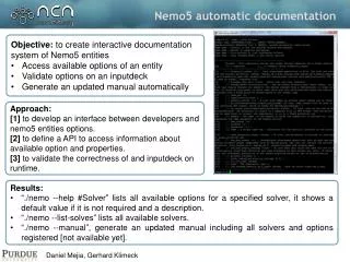
Using NEMO5 to quantitatively predict topological insulator behaviour. Parijat Sengupta , Tillmann Kubis , Michael Povolotskyi , Jean Michel Sellier , Jim Fonseca, Gerhard Klimeck

E N D
Using NEMO5 to quantitatively predict topological insulator behaviour ParijatSengupta, TillmannKubis, Michael Povolotskyi, Jean Michel Sellier, Jim Fonseca, Gerhard Klimeck Network for Computational Nanotechnology (NCN)Electrical and Computer EngineeringPurdue University, West Lafayette IN, USA Summer School 2012
Some commonly known facts * *Wikipedia
A dispersion cartoon Conduction band Eg Valence band An insulator such as SiO2, Si3 N4 with large band-gap • Conduction and Valence bands describe electrons and holes • The band gap is zero in a metal • Some materials possess the dual properties of metals and insulators • We will use NEMO5 to investigate some of these unique materials
What are these materials? Dispersion obtained through ARPES* sp3d5s* tight binding calculation Dirac Cone *Rev of Mod. Phys, Vol 82, Oct-Dec 2010 ε • Primary examples are Bi2Te3 , Bi2Se3 , BixSb1-x etc… • They are known as topological insulators • These materials contain bound surface states κ
Setting up the simulation task sp3d5s* tight binding calculation • We will use a sp3d5s* tight binding model • Bi2Te3 is our topological insulator material • A 9 nm (appx) long quantum well will be the target device • This will produce a band structure as shown on left Dirac Cone Key feature of this dispersion is a graphene-like linear character (Dirac cone) Linearity is not due to same reason as in graphene!
Details of the simulation structure 9 nm wide c-axis oriented Bi2Te3 thin film Z-axis : Confined X & Y axes : Periodic Bi terminated surface Bi periodic Te1 Te2 periodic Te terminated surface Different surface termination: Surface 1 (2) is Bi (Te2) terminated
The NEMO5 input deck skeleton There are 3 blocks in the input deck: Structure { } Defines material and simulation domains Solvers { } Sets up simulations that has to be solved, e.g. equations, boundary conditions, iterative processes, output, numerical options, etc. Global { } Defines global variables such as temperature, which database file to use, diagnostic output, etc.
The NEMO5 input deck: The first block “Structure” Structure { } Material { name = XYZ … } Material { name = ABC … } Domain { name = device … } Domain { name = contact1 … } Geometry { } Materials Domains for simulations Description of the geometry
Setting the input deck… • Every input deck begins with the Structuregroup • Each region is identified by a name known as the tag • The underlying crystal structure of the material needs to be provided • Each simulation can have multiple regions, NEMO5 needs the exact number of those for correct execution • The surface atoms can be controlled by asking NEMO5 to place a specific atom when constructing the first unit cell
Defining parameters and the domain • Any parameter defined in the input deck takes precedence over the corresponding database entry • Dimension creates a canvas of unit cells • Periodicity set as false refers to a confined axis k is not a good quantum number • Passivateoptions allows inclusion of Hydrogen atoms
Crystal orientation in NEMO5 • Crystal directions set up the coordinate system within the crystal using the basis vectors • The basis vectors are aligned to the Cartesian axes through the space orientation option • In this example: crystal_direction1 = (0,0,1) is aligned along space_orientation_dir1 = (0,0,1) or the z-axis. • You need to specify only 2 directions. N5 computes the third using the crystal structure info. space_orientation_dir1 is the z-axis and is confined: the first entry of periodic option
“crystal_direction” & “space_orientation”: A closer look • What NEMO5 internally produces ? • It produces three basis vectors • These basis vectors can be obtained by examining the first three lines of the device_coupling.dat file • To obtain this file, include output = (xyz, coupling) in the Domain section. You will see an example of it in your first exercise Three vectors in the device_coupling.dat file a = [0 0 3.0487] b = [0.4383 0 0] c = [-0.2191 0.3796 0] How do you check that these vectors make sense? All length units are in nm
Reconciling results to known crystal geometry • Our test case here is Bi2Te3 which has a hexagonal base • Each edge of hexagon is 0.4383 nm • Two hexagons are displaced along z-axis by 3.0487 nm c Three vectors in the device_coupling.dat file a=[0 0 3.0487] b= [0.4383 0 0] c = [-0.2191 0.3796 0] b • Hexagonal base of Bi2Te3 quintuple layer • The vectors b and c have an 120 degree angle between them Check: • Norm of vectors b and c is equal to 0.4383 nm • Norm of vector a is equal to 3.0487 nm • Angle between b and c is 1200 as expected
The actual geometry in numbers • Shape options allows you to input a geometric shape for your device • Setting the priority gives you control over structure creation when dealing with composite geometric shapes. • Higher priority gets constructed first • Actual device size is specified through min & max
The NEMO5 input deck skeleton There are 3 blocks in the input deck: Structure { } Defines material and simulation domains Solvers { } Sets up simulations that has to be solved, e.g. equations, boundary conditions, iterative processes, output, numerical options, etc. Global { } Defines global variables such as temperature, which database file to use, diagnostic output, etc.
Executing the input deck: The solvers! • Each solver has a name • The first solver (usually) is the geometry constructor • The atomic coordinate positions are dumped out in a structure file • The structure file can have several formats such as vtk, silo, xyz, pdb…
Electronic structure calculation options - I • Electronic structure calculation must set the type to Schroedinger • job_list shows what actions N5 must perform • Setting orbital_resolved to true shows the contribution of each orbital to overall band structure
Electronic structure calculation options - II • tb_basis option lets you choose the band structure calculation model. • tb_basis can also be set to effective mass (em) • k_space_basis can also be set to Cartesian • Number of nodes Number of k-points in the chosen k interval
The NEMO5 input deck skeleton There are 3 blocks in the input deck: Structure { } Defines material and simulation domains Solvers { } Sets up simulations that has to be solved, e.g. equations, boundary conditions, iterative processes, output, numerical options, etc. Global { } Defines global variables such as temperature, which database file to use, diagnostic output, etc.
Putting it all together… • The global section has the command solve: All job names are included under solve • database is custom built for N5 and contains all material parameters • messaging level indicates code progress output on screen. Level 5 is verbose
Exercise -I • Log in to your workspace account and create a folder TI in your home directory. Navigate to the TI folder • mkdir TI • cd TI • Pull the necessary files in your TI folder by typing the following : • cp ../public_examples/NCN_summer_school_2012/ • Topological_Insulators_psengupta/ex*.in . • cp ../public_examples/NCN_summer_school_2012/ • Topological_Insulators_psengupta/spin_analysis_ex*.m . • ex1.in is the input file to calculate the dispersion relationship for a 9.0 (appx) long Bi2Te3 quantum well • Submit a job by typing the command : • submit -v ncn-hub@coates -i ../all.mat -n 16 -N 8 nemo-r8028 ./ex1.in
What do you expect to see as a solution? • NEMO5 will produce four files (SS12_TI_ex1_*.dat) • Start MATLAB on your workspace • Your folder has a MATLAB file called spin_analysis_ex1.m • Execute the MATLAB script by typing spin_analysis_ex1 at the command prompt • You will have the figure on your left! Band structure for a 9.0 nm long Bi2Te3 quantum well To run Matlab: $ use matlab-7.12 $ matlab
Exercise –I contd… Pre-computed results are stored in folder /public_examples/NCN_summer_school_2012/Topological_Insulators_psengupta • Supplementary exercise : • Change line 20 of the spin_analysis_ex1.m file from the preset • n = [1 0 0] to n = [0 0 1] and n = [0 1 0] • Run Matlab • The three different spin-polarized plots that you obtain highlight a fundamental theory of TIs
Inter-linking solvers in NEMO5 Several solvers defined in the Solver block can be inter-linked: Solver1 { } Solver2 { } We will see a specific example of this coupling of solvers in the next part of the tutorial Solver3 { }
NEMO5 is a toolbox…. Start solve = (struct, schrödinger, poisson) Density solver (e.g. Schrödinger) Update ɸ Potential solver (e.g. Poisson (ɸ)) No Yes Conv ? End • Solvers can also speak to one another • e.g. A self-consistent charge calculation
Setting up the Poisson… • A name is assigned to the Poisson solver (similar to previous slides) • A non-linear Poisson will be solved • A continuum domain is constructed • Linear solver settings • Electrostatic output option
Linking Poisson to Schroedinger… • Specific model applicable to topological insulators • Convergence criterion • The simple linking step done through inserting name of desired solver • job_list tells NEMO5 to compute specific physical quantities • For a self-consistent calculation electron density is computed
A few options in the density solver • First two blocks of input statements are identical to normal eigen value calculations done earlier • threshold_energy lets you choose eigen states beginning with energy as set in the option • chem_pot is the Fermi level to start calculations • Schrodinger receives the potential from the my_poissonpotential solver Inter-linking solvers : my_poisson and BiTe_density More advanced calculations can use boundary condition options
Implementing boundary conditions • Boundary conditions can be of two forms in NEMO5. • Dirchlet (potential (ɸ) = constant) • Neumann (∂ɸ = constant) • The input deck statements shown on left can be included multiple times at all possible external boundaries • The right boundary region number must be specified • E_field allows to apply an electric field of certain magnitude to device structure. It is in units of V/cm
Updating Schrödinger for eigen states calculation • Exactly same format as in Exercise 1 • Potential solver is added which supplies potential to the tight - binding Hamiltonian
Exercise -II • ex2.inis the input file to calculate charge self-consistent dispersion relationship for a 9.0 (appx) long Bi2Te3 quantum well • This task will produce a dispersion relationship, potential landscape, and the charge profile in the device • Submit the job by typing the command : • submit -v ncn-hub@coates -i ../all.mat -n 16 -N 8 nemo-r8028 ./ex2.in
What do you expect to see as a solution? • NEMO5 will produce four .dat files (SS12_TI_ex2_*.dat) and a .xy file (poisson_ex2.xy) • Start MATLAB on your workspace • Your folder has a MATLAB file called spin_analysis_ex2.m • Execute the MATLAB script by typing spin_analysis_ex2at the command prompt • You will have the figure on your left! Self-consistent band structure for a 9.0 nm long Bi2Te3 quantum well
Electrostatic calculations • Use the poisson_ex2.xy file (three column file) in your folder to plot the charge and potential profile • Start MATLAB on your workspace • Type the following for the charge & potential plot : • cp = load(‘poisson_ex2.xy’); • % potential plot • figure(1) • plot(cp(:,1), cp(:,2)) • % charge plot • figure(2) • plot(cp(:,1), cp(:,3)) You can also use any plotting software : Please remember : Column 1 is device coordinate followed by potential and charge data on columns 2 and 3
How do the results from Exercise I and II look like? Self-consistent electronic structure Schrödinger 20 band tight binding • Poisson calculation has large impact: • Energy separation between Dirac cones gets enhanced • Fermi velocity of Dirac states changes (mobility) • Dirac points move below the Fermi level, into the bulk DOS
Self-consistent electrostaticcalculations Bi terminated surf. Intrinsic dipole due to distinct surfaces Common in TB: Charge oscillations between atom types Te terminated surf. • Smooth perturbative potential • Oscillations in the potential between anion/cation covered by bulk parameters • Change of charge polarity at two surfaces due to different atomic termination
Conclusion • Band structure calculations • Can handle the newest materials like topological insulators • Charge self-consistent band structure calculation • For accurate device prediction • Use of solvers to accomplish modular tasks • As many solvers as needed can be added • Solvers can be inter-linked • Simple process accomplished by inserting appropriate solver name Thank you.