Download
1 / 18
180 likes | 290 Vues
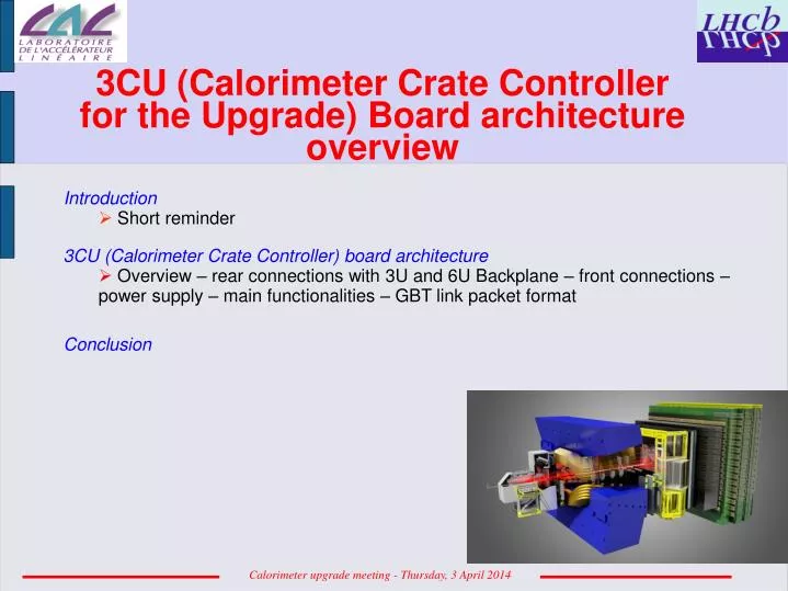
3CU ( Calorimeter Crate Controller for the Upgrade) Board architecture overview. Introduction Short reminder 3CU (Calorimeter Crate Controller) board architecture

E N D
3CU (Calorimeter Crate Controller for the Upgrade)Board architecture overview • Introduction • Short reminder • 3CU (Calorimeter Crate Controller) board architecture • Overview – rear connections with 3U and 6U Backplane – front connections – power supply – main functionalities – GBT link packet format • Conclusion
Introduction : short reminder • Front-end crate with same backplanes and power supply • 3U power supply, clock distribution, … • 6U links between boards inside the same crate • New Front-end board with optical link DAQ and LLT. • New Control Board (3CU) • Remove TVB • Calorimeter Crate Controller board • Ensure signal distribution inside Front-end crate • Clock distribution from the CROC to all front-end board inside the same crate through backplane • Slow control through 6U backplane • Fast command (BxId Reset, FE Reset, …) through 3U backplane • Crate Power supply • Reused Marathon equipment
3CU Board : Preliminary architecture DC-DC Converter 2V5 -> Vcc IO DC-DC Converter 2V5 -> 1V2 DC-DC Converter 2V5 -> 1V5 Rear Front B25 Buffer Buffer 60x4,6k RAM block E-Port Prim. / Second. 1V2 6 x CCC (Clock Conditioning Circuit) PS: 3V3 PS: 3V3 tbd A3PE1500 Slow Control distribution to FEB through 6U_backplane tbd VCC Core Network Controller USB Interface USB USB VCC I/O_1 16 FEB Delatching Ctrl line Ref_Clk[0:7] VCC I/O_2 AB25 Delatching Ctrl. In_Ext_Clk E-Port (TTC_cmd) Clk Ref / PLL Phase Shifter TTC command E-Port Clk Manager SLVS / LVDS Translator E-Port VTRx LVDS User Buses : TOSA GBLD {I2C, //, SPI, JTAG, 12bADC, …} TTC cmd GBT-SCA Laser Diode E-Port_SC_FEB Edge-connector SLVS / LVDS Translator I2C LVDS Slow control to FEB Uplink PD +GBTIA E-Port OnBoard_Clk PCB Diff. Signal: Clk, DOUT, DIN E-Port ROSA Slow Ctrl Ext_Clk E-Port Out_Ext_Clk B25 General Ctrl Crate_Clk Out_1 Down-link LEMO …….. x (16) Clock Conditioning Circuit Dedicated Clock IO Out_2 Dedicated Clock IO Ref_Clk[0] LVDS In_Ext_Clk 444 Max user I/Os – 8 I/O Banks I2C Master In_1 LEMO In_2 GBTX Clock distribution to FEB through 3U_backplane In_1 In_2 Out_1 Out_2 In_Ext_Clk Out_Ext_Clk E-Port_SCA AB25 TTC cmd distribution to FEB through 3U_backplane 1 Bi-directionnal link TTC command Protocol used on the board Power Supply: B77 80b @ 40MSPS 2V5 / 100A 3V3 / 100A
Clocktree • Clock tree of the 3CU board: • The clock is provided by the GBTx Chip • On the 3CU board we will multiplex the clock with Ext_Clk and On_Board_CLK Ext_Clk (debug) Crate_Clk On_Board_Clk GBTx_Clk Sel • Clock multiplexing several ways possible • Multiplexing inside A3PE FPGA: • For dedicated Clk_IO • Clk_IOtPY # 0.9 ns • (Pad to data delay through the input buffer with Schmitt trigger disable) • Clock Conditioning Circuit (CCC) • Low output jitter: worst case < 2.5% × clock period peak-to-peak period jitter when single global network used : # 625 ps • Multiplexing with discret components • Necessity to use radhard components • Other solution: • Same problem on ATLAS ( see Stefan Simion)
Slow control to FEB through 6U backplane (3 differentials pairs between Control slot and each FEB) 6U Backplane 3CU Board : rear connection with 3U and 6U Backplane Rear Delatching control (1point to point connection between each FEB and Control board) B25 3CU Board Buffer Buffer Crate Id (8 bit DIP switch on 6U_backplane) Connected to 6U backplane PS: 3V3 PS: 3V3 AB25 Buffer Slow control to FEB B25 Current 3U Backplane power supply: Current 3U SPECS Bus connection: Clock distribution from Control board to all slot of the same crate (20 differentials pairs between Control slot and each FEB) Crate_Clk 3U Backplane AB25 TTC[8:0] Timing Trigger and Control command TTC command Slot ID (4 bit ….) 2V5 / 100A Connected to 6U backplane 3V3 / 100A -5V ?? B77 Vfree_2 Vfree_1 Tbd Tbd
3CU Board : front connections Front USB Interface USB Ref_Clk[0:7] In_Ext_Clk Clk Ref / PLL Phase Shifter E-Port Clk Manager E-Port VTRx TOSA GBLD Laser Diode Edge-connector I2C Uplink PD +GBTIA E-Port PCB Out_Ext_Clk Diff. Signal: Clk, DOUT, DIN E-Port ROSA Out_1 LEMO E-Port General Ctrl Out_2 Down-link …….. In_Ext_Clk In_1 LEMO GBTIA NIM ?? I2C Master In_2 GBTX NC7SZ125 ? 1 Bi-directionnal link 80b @ 40MSPS GBLD ROSA: Receiver Optical Sub Assembly TOSA: Transmitter Optical Sub Assembly
GBT- Power Supply VTRx power supply: GBT-SCA power supply: 1V2 GBLD : Vdd 2V5 GBTIA: Vdd1=2V5 ; Vdd2 =1V5 GBTX power supply: 1V5 GBT-SCA footprint: - 144 pin CSP BGA (Chip Scale Ball Grid Array) package - Size of the package 10x10mm with a ball pitch of 0.8mm Digital, Clock manager,Digital IO, phase shifter, receiver, tranceiver E_fuse power 3V3 during programming 1V5 otherwise !! GBTX footprint: • matrix 20x20 0.8 mm pitch - Size 17x17 mm
GBT-linkPacket Format • Fixed packet length: 120bits • Packet transmission rate: 1/25ns • Data transmission rate: 4.8 Gbps • Fixed bandwidth allocation: • Trigger path: 640 Mbps • Control path: 160 Mbps • 1 internal e-link (for GBT management) • 1 external e-link (for GBT-SCA chip) • Data path: 2.56 Gbps • 32 e-links @ 80 Mbps • Data flow: • Transmission of GBT-packets is continuous • Data from e-link ports are muxed/demuxed in the GBT-link stream • GBT data path is unaware of the e-link transfer protocol.
GBT-linkPacket Format Mapping of the GBT “frame” on the e-port 16-bit TTC command Only 8 decoded on the Control board and transmit to the FEB Header field (H) : A 4-bit header field is transmitted at the beginning of each frame. Slow Control information (4-bit): Internal Control (IC 2-bit) and External Control (EC 2bit) The 2-bit IC control field is used to control and monitor the GBTX operation. The 2-bit External Control (EC) field has an associated bandwidth of 80 Mb/s and it is part of the slow control channel. Although intended to implement a slow control channel (e.g. for the GBT-SCA) Data field (Data) The 80bit data field is used for generic transmission of data, having an associated bandwidth of 3.2 Gb/s. The data field is fully available to the user via the flexible E-links and is fully protected by the FEC. Forward Error Correction field (FEC) The 32-bit FEC field is used to protect all the other fields in the frame against transmission errors due to link noise and single event upsets.
Conclusion : Pending questions • Verify the compatibility SLVS LVDS (TullioGrassi !) • Choice of the Clock multiplexing • Jitter acceptable at the input of the GBTx on the Front-End Board ? • Choice of the FPGA target (A3PE or IGLOO2 ?). The idea is to use the same target of the FEB, if is it possible ? • Disponibility of the GBT_SCA • End of the year (optimistic ! ) • Alternative solution, integration of the SCA core in the FPGA • Used of the NIM IN/OUT or other standard (-5V ?)
GBT SCA A3PE IGLOO2
GBT SCA IGLOO2 A3PE
Radiation Hard Optical Link Architecture GBT GBT Versatile Link FPGA Timing & Trigger Timing & Trigger GBTX PD GBTIA DAQ DAQ LD GBLD Slow Control Slow Control Custom ASICs On-Detector Radiation Hard Electronics Off-Detector Commercial Off-The-Shelf (COTS)
Paulo.Moreira@cern.ch The GBT System External clock reference FEModule Clock[7:0] E – Port e-Link GBTX Phase - Shifter CLK Reference/xPLL E – Port FEModule E – Port ePLLRx GBTIA DEC/DSCR CDR E – Port data-down data-up Phase – Aligners + Ser/Des for E – Ports CLK Manager clock 80, 160 and 320 Mb/s ports GBLD SCR/ENC SER E – Port ePLLTx FEModule E – Port E – Port One 80 Mb/s port Control Logic Configuration (e-Fuses + reg-Bank) GBT – SCA JTAG I2C Slave I2C Master E – Port I2C (light) data JTAG Port I2C Port control clocks
GBT SCA • ASIC dedicated to slow control functions. • System Upgrades for SLHC detectors. • Replacement for the CCU & DCU ASICs(Communication Control Unit & Detector Control Unit in CMS). • It will implement multiple protocol busses and functions: I2C, JTAG, Single-wire, parallel-port, etc… • It will implement environment monitoring and control functions: • Temperature sensing • Multi-channel ADC • Single channel DAC • Flexible enough to match the needs of different FE systems. • Technology: CMOS 130nm using radiation tolerant techniques. SCA 16xI2C buses JTAG master Slow Control e-link Single Wire bus * Network Controller RXDATA e-port TXDATA 4x digitalI/O Ports 4 Memory Bus (8b) 8 TEMP ADC8-16 inputs DAC ALARMs * advance information Kostas.Kloukinas@cern.ch
SLVS standard • SLVS (Scalable Low Voltage Standard) • JEDEC standard: JESD8-13 • Differential voltage based signaling protocol. • Voltage levels compatible with deep submicron processes. • Typical link length runs of 30cm over PCB at 1Gbps. • Low Power, Low EMI • Application in data links for Flat Panel displays in mobile devices. • Mobile Pixel Link, MPL-2 (National semi.) LVDS 400mV SLVS specifications brief 2 mA Differential max Line impedance: 100 Ohm Signal: +- 200 mV Common mode ref voltage: 0.2V 1.2V SLVS 200mV 0.2V