Download

1 / 19
190 likes | 413 Vues
ADC and DAC. Reason for Signal Conversion. AD2 DA1. digital. Topics. Analog to Digital Conversion Digital to Analog Conversion. Analog to Digital Conversion. Digilent’s PMODAD2. Schematic of PMOD AD2. PMODAD2 uses AD7991 from Analog Devices. Successive Approximation ADC.

E N D
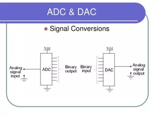
Reason for Signal Conversion AD2 DA1 digital
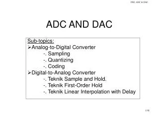
Topics • Analog to Digital Conversion • Digital to Analog Conversion
Schematic of PMOD AD2 PMODAD2 uses AD7991 from Analog Devices
Successive Approximation ADC The analog input voltage (VIN) is held on a track/hold. The N-bit register is first set to midscale (that is, 100... .00, where the MSB is set to 1). This forces the DAC output (VDAC) to be VREF/2. A comparison is then performed to determine if VIN is less than, or greater than, VDAC. If VIN is greater than VDAC, the comparator output is a logic high, or 1, and the MSB of the N-bit register remains at 1. Conversely, if VIN is less than VDAC, the comparator output is a logic low.
Successive Approximation ADC 3. The SAR control logic then moves to the next bit down, forces that bit high, and does another comparison. The sequence continues all the way down to the LSB. 4. Once this is done, the conversion is complete and the N-bit digital word is available in the register.
Graphical Illustration The y-axis (and the bold line in the figure) represents the DAC output voltage. In the example, the first comparison shows that VIN < VDAC. Thus, bit 3 is set to 0. The DAC is then set to 01002 and the second comparison is performed. As VIN > VDAC, bit 2 remains at 1. The DAC is then set to 01102, and the third comparison is performed. Bit 1 is set to 0, and the DAC is then set to 01012 for the final comparison. Finally, bit 0 remains at 1 because VIN > VDAC.
Signal Conversion (1) (-Vin)
Signal Conversion (2) (-Vin+VREF/2) The comparator output yields a logic 1 if VCOMMON < 0 (i.e., VIN > ½ × VREF). The comparator output yields logic 0 if VIN < ½ × VREF. If the comparator output is logic 1, then the bottom plate of the MSB capacitor stays connected to VREF. Otherwise, the bottom plate of the MSB capacitor is connected back to ground.
Signal Conversion (3) (-Vin+VREF/2) This slide assumes that MSB is a 1. In general, VCOMMON = -VIN + BN-1 × VREF/2 + BN-2 × VREF/4 + BN-1 × VREF/8 + ... + B0 × VREF/2N-1
R2R 3-Bit Digital to Analog Converter 741 Op-Amp Chapter 5