Download
1 / 24
250 likes | 455 Vues
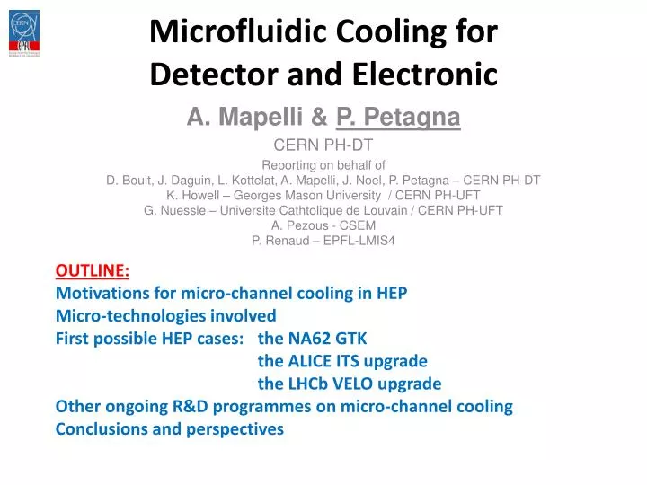
A. Mapelli & P. Petagna CERN PH-DT Reporting on behalf of D. Bouit , J. Daguin, L. Kottelat, A. Mapelli, J. Noel, P. Petagna – CERN PH-DT K. Howell – Georges Mason University / CERN PH-UFT G. Nuessle – Universite Cathtolique de Louvain / CERN PH-UFT A. Pezous - CSEM

E N D
A. Mapelli & P. Petagna • CERN PH-DT • Reporting on behalf of • D. Bouit, J. Daguin, L. Kottelat, A. Mapelli, J. Noel, P. Petagna – CERN PH-DT • K. Howell – Georges Mason University / CERN PH-UFT • G. Nuessle – UniversiteCathtolique de Louvain / CERN PH-UFT • A. Pezous - CSEM • P. Renaud – EPFL-LMIS4 Microfluidic Cooling for Detector and Electronic OUTLINE: Motivations for micro-channel cooling in HEP Micro-technologies involved First possible HEP cases: the NA62 GTK the ALICE ITS upgrade the LHCb VELO upgrade Other ongoing R&D programmes on micro-channel cooling Conclusions and perspectives
Twepp 2009 (Paris): J.R. Thome, J.A. Olivier, J.E. Park Two-Phase Cooling of Targets and Electronics for Particle Physics Experiments • Main focus: high power densities, up to as high as 350 W/cm2; • However, interesting preliminary features also for HEP applications; • State-of-the-art heat transfer and pressure drop models presented; Motivations I : starting point Geometry sensitivity for liquid cooling Silicon m-channel cooling device used for testing at EPFL Typical laboratory fluid distribution! Liquid vs. evaporative Channel parameters used for Thome’s preliminary simulations based on the NA62 GTK test case
MINIMIZATION OF MATERIAL BUDGET • ultra thin Si cooling plates and tiny (PEEK?) pipes • no mechanical components required for thermal bridges • COOLING POWER ENHANCEMENT • very high heat transfer coefficients (very small Dh) • very high heat flux (large S) • REDUCTION OF DT BETWEEN HEAT SOURCE & HEAT SINK • large surface available for the heat exchange (cold plate vs. cold pipe) • natural minimization of the thermal resistance between the source and the sink Fluid thermal conductivity 0.05 ÷ 0.11 Laminar flow 3.66 ÷ 4.36 Motivations – II : advantages for HEP O (103 W/m2K) O (10-4)
Examples of cooling solutions in LHC trackers Lower temperatures are envisaged for the future Si-trackers at SHLC. This has non-negligible technical impacts on the cooling plants With a standard cooling approach, the DT between the module and the fluid ranges between 12 and 20 C (small contact surface + long chain of thermal resistances) Motivations – III : thermal performance Pix Strip DT ~ 15 C Thermal contact & Heat spreader Substrate Heat sink DT ~ 10 C ATLAS IBL staves Si sensor Carbon foam + CFRP skin Si chips DT ~ 5 C Cooling pipe Si cold plate Adhesive NO CTE DIFFERENCE!
Present LHC large Si trackers (ATLAS and CMS) ~ 2% X0 per layer SLHC “phase II” upgrade: “significant” reduction needed Future trackers at ILC ~ 0.1 ÷ 0.2% X0 per layer Motivations – IV : impact on material budget X/X0 vs. h for the CMS Si-strip Tracker X/X0 vs. h for the CMS PIX detector PANDA %X0 %X0
Microfabrication technologies are derived from microelectronics to fabricate microsystems and microfluidic devices. Fully laminar flow ensures high degree of predictability and control No sources of instabilities and/or vibrations Micro Fabrication Technologies Weigl & Hedine, Am. Biotech. Lab., 2002, 20, 28-20 Bulk micromachining: mechanical structures are etched in the wafer. Surface micromachining: layers of material are deposited on the wafer and structured. Commonly used substrates and materials include Silicon, SOI, Glass, Pyrex, Quartz, Polymers (SU-8, Polyimide, Parylene), Metals,...
Etching of microchannels • Dry Etching • Plasma, RIE, DRIE • Wet Etching • Chemical: KOH, TAMH, PGMEA Micro Fabrication: Etching • Silicon KOH • Walls depend on crystal orientation • SU-8 photoresist • Vertical walls • Silicon DRIE • Anisotropic, vertical walls
Direct Bonding • Silicon Fusion Bonding • Si-Si, Si-SiO2 • Annealing ~1000°C • Optional tool pressure • Plasma-activated • Low temp. • Required: - wafer flatness • - Surface roughness < 1 nm • Anodic Bonding • Pyrex-Si, Si-Pyrex-Si • Temp. ~400°C • Voltage 50 ÷ 1200 V • Tool pressure • Intermediate layer bonding • Polymers (SU-8, Parylene,…) • Thermocompression • Eutectic (AuIn, AuSn, AuSi, AlGe..) • Glass Frit Micro Fabrication: Bonding
Wafer thinning Grinding Chemical Mechanical Polishing Etching Micro Fabrication: Thinning Local thinning Etching (dry or wet)
m-channel cooling plate • Final target: 0.10 – 0.15 % X0 • (Silicon thickness < 150 mm) • 3 INDEPENDENT STATIONS: “SIMPLE” SYSTEM “Keep it simple at first” approach: liquid C6F14 cooling Design optimization Wedged manifold, 1.6 mm Max width, 150 mm thick Wedged manifold, 1.6 mm Max width, 280 mm thick Wedged manifold, 1.6 mm Max width, 400 mm thick NA62 GTK – Requirements and Basic Concept • Priority: minimize X0 • Acceptable DT over sensing area ~ 5 °C • Dimension of sensing area: ~ 60 x 40 mm • Max heat dissipation: ~ 2 W/cm2 • Target T on Si sensor ~ -10 °C
Wall thickness between channels: 200mm (for Si fusion bonding) or 50mm (for Si-Si anodic bonding) NA62 GTK – Details of m-channel Design Manifolds 280 µm deep Max width = 1.6 mm Through holes • Channels: 100 x 100 µm Channels: 100 ÷ 300 µm wide 100 ÷ 70 µm deep manifolds channels NA62 baseline design holds ~ 20 bars. Critical point at the level of the manifold’s maximum width (1.6 mm). Safety factor: 3 to 5
Connectors NA62 GTK –m-channel Thermal Performance Outlet 1 2 3 4 5 Heater 1 6 7 8 10 10 6 8 9 9 7 11 13 12 Heater 2 15 14 15 13 14 11 12 Wafer equipped with GTK simulator Heater 3 Inlet Max DT on sensor ~ 6 C Fluid-sensor DT ~ 6 C 6 10 8 9 7 11 13 12 14 15
Dual inlet / dual outlet design allows for more uniform flow distribution and for sensible pressure drop reduction 100 ÷ 240 Influence of channel geometry on total pressure drop IN IN 480 ÷ 760 150 70 280 NA62 GTK –Second Order Optimization Thinning by grinding Thinning by selective etching 100 ÷ 240 200 A second round of CFD and structural parametric analysis brings to a fully compliant solution: now submitted to the collaboration for approval OUT OUT manifolds channels Drawing not to scale All dimensions in µm Limit of acceptance
Stave from SPD to ITS ALICE ITS –First Approach ~ 200 mm Sketch of building blocks constituting a generic stave Conventional configuration Micro-channel cooling approach • Two working possibilities: • evaporative C4F10 • monophase water in underpressure
Common return pipe Module n+1 ALICE ITS –Sideline Micro Channels? Sketch of building blocks constituting a generic stave ~ 0.5 W/cm2 Sideline micro-channels No power dissipation Common Inlet pipe Module n Remove silicon cooling plate where not needed hole
ALICE ITS –Open Issues ~ 200 mm Sketch of building blocks constituting a generic stave • Long stave (~ 200 mm): • multi-module m-channel solution? (multi connector or module-to module junction) • Single m-channel from 12” wafer? (higher cost and more difficult handling of thinned devices) • “Packed” barrel configuration” • Need for a reliable in-plane m-connector. Discussions ongoing with CSEM for a common R&D programme ?
Power dissipated: ∼2 W/cm2 Cooling: evaporative CO2 Cooling substrate in acceptance: 250 ÷ 500 μm out of acceptance: ∼1 mm LHCb VELO –First Approach Baseline configuration Out of acceptance up to 1 mm Si! Micro-channel configuration CO2 saturation pressure at room temperature: high pressure is not an issue!
LHCb VELO –Open Issues Small issue: Out-of plane connector is acceptable, but a special reduced size production must be requested (Nanoport connectors rated up to 103 bar!) Big issue: LHCb VELO is inside the secondary LHC vacuum: absolute reliability is required!!! Main problem: QA/QC of the hermetic bond between the two wafers
EPFL: Thome, Atienza, Leblebici ETHZ: Poulikakos IBM: Michel, Brunschwiller Other R&D Programmes –CMOSAIC “The CMOSAIC project is a genuine opportunity to contribute to the realization of arguably the most complicated system that mankind has ever assembled: a 3D stack of computer chips with a functionality per unit volume that nearly parallels the functional density of a human brain. CMOSAIC's aggressive goal is to provide the necessarily 3D integrated cooling system that is the key to compressing almost 1012 nanometer sized functional units (1 Tera) into one cubic centimeter with a 10 to 100 fold higher connectivity than otherwise possible”
Other R&D Programmes –Polyimide m-channels Courtesy of I. Sgura and C. Pastore (INFN Bari)
Other R&D Programmes –Polyimide m-channels Courtesy of I. Sgura and C. Pastore (INFN Bari)
Other R&D Programmes –Polyimide m-channels Courtesy of I. Sgura and C. Pastore (INFN Bari)
Micro-channel cooling features highly interesting potentialities for HEP applications Available m-technologies allow for a palette of solutions adapted to different requirements and specific environments A working solution for the NA62 GTK is ready for submission to the experiment Activities for the ALICE ITS and for the LHCb VELO upgrades have started Parallel activities are ongoing outside CERN for hi-power computing (IBM, EPFL, ETHZ) and for HEP (Bari/CERN Polyimide m-channels for ALICE ITS) m-channel cooling is perfectly suited for future 3D architectures (if any...) Main issues to be addressed: Reliable QA/QC process for hermetically sealed channels (bonding) Reliable miniaturized in-plane connections Conclusions
PHASE I: m-channel cooling plates conceived to adapt to an existing electronics design and placed in good thermal contact (NA62 GTK) Perspectives for m-channels in HEP PHASE II: m-channel cooling plates conceived in connection with the electronics design and integrated at the same time in the module’s architecture (maybe already possible with ALICE and LHCb phase I upgrades) PHASE III: m-channel cooling integrated in the module conception: In the sensor? Compatible with physics performance? In the chips? When? By whom? In the Si-Interposer? (should 3D become real...)