Download
1 / 17
170 likes | 354 Vues
COSMOS Summer 2008 Chips and Chip Making. Rajesh K. Gupta Computer Science and Engineering University of California, San Diego. Roadmap. Topic: Integrated circuit chips This lecture IC Chips, Chip making ingredients and steps. Reference

E N D
COSMOS Summer 2008Chips and Chip Making Rajesh K. Gupta Computer Science and Engineering University of California, San Diego. 2008 R. Gupta, UCSD
Roadmap Topic: Integrated circuit chips This lecture IC Chips, Chip making ingredients and steps. Reference “How chips are made” – Intelhttp://www.intel.com/education/makingchips/index.htm “Microelectronics 101” – IBMhttp://www-306.ibm.com/chips/technology/makechip Keywords: • 2008 R. Gupta, UCSD
The Chip: A Packaged Part Quad Flat Pack (QFP) Ball Grid Array (BGA) http://education.netpack-europe.org/chipp.php
The Die Under a Microscope Intel 4004 (‘71) Intel 8080 Intel 8085 Intel 8486 Intel 8286
A Gate Layout Defines a set of “masking layers” for printing purposes.
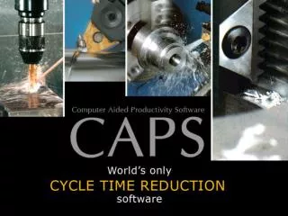
The Ingredients Silicon Wafers cut from an ingot of pure silicon. Chemicals and gases are used throughout the chip-making process. Metals, such as aluminum and copper, are used to conduct the electricity throughout the microprocessor. Gold is also used to connect the actual chip to its package. Ultraviolet (UV) Light has very short wavelengths and is just beyond the violet end of the visible spectrum. Masks used in the chip-making process are like stencils. When used with UV light, masks create the various circuit patterns on each layer of the chip. [Courtesy Intel. Adapted from http://www.intel.com/education/teachtech/learning/chips/preparation.htm]
Building Chip Start with a disk of silicon called wafer 75 mm to 300 mm in diameter, < 1 mm thick cut from ingots of single-crystal silicon pulled from a crucible of pure molten polycrystalline silicon using a seed crystal Different processing steps and techniques Introduce dopants Oxidation Masking Polysilicon
Introduce Dopants Pure silicon is a semiconductor bulk electrical resistance in between that of a conductor and insulator Conductivity of silicon can be varied several orders of magnitude by introducing impurity atoms called dopants acceptors: accept electrons to leave holes in silicon lead to p-type silicon (e.g. Boron) donors: provide electrons to silicon lead to n-type silicon (e.g. Arsenic, Phosphorous)
Introduce Dopants (2) Deposition through diffusion evaporating dopant material into the silicon surface thermal cycle: impurities diffuse deeper into material Ion Implantation silicon surface subjected to highly energized donor or acceptor atoms atoms impinge silicon surface, and drive below it to form regions of varying concentrations Ion Implantation
Oxidation Method 1: Heating silicon wafers in an oxidizing atmosphere (O2 or H2O) Consumes Si Grows equally in both vertical directions Method 2: Deposition Deposited on top of existing layers
Masking Masks act as barrier against e.g. ion implantation dopant deposition before diffusion (dopants do not reach surface) oxidation (O2 or H2O does not reach surface) Commonly used mask materials photoresist polysilicon silicon dioxide (SiO2) silicon nitride (SiN)
Example: oxide mask • bare silicon wafer • oxidize wafer • deposit layer of photoresist • expose the photoresist selectively to UV light • The drawn mask pattern determines which part is exposed • Resist polymerizes where exposed
unexposed resist is removed with solvent: negative resist • (positive resist: exposed resist is removed) • exposed oxide is etched • photoresist is washed off • the oxide can now be used as a masking layer for ion implantation
The Printing Challenge • UV lithography: line width limited by diffraction and alignment tolerances, but tricks are used • Electron beam lithography has emerged: directly from digital data, but more costly and slow
Polysilicon Silicon also comes in a polycrystalline form called polysilicon, or just poly high resistance normally doped at the same time as source/drain regions Used as an interconnect in silicon ICs gate electrode in MOS transistors most important: acts as a mask to allow precise definition of source and drain extension under gate minimum gate to source/drain overlap improves circuit performance (why?) called self-aligned process
Packaging Single die Wafer From http://www.amd.com