Download
1 / 62
620 likes | 640 Vues
This review discusses the details of cache memory and its hardware structure in computer systems, with references to relevant textbooks. The objective is to familiarize students with cache memory and its application in computer architecture. The review also highlights the importance of reducing the processor-memory speed gap.

E N D
Review of Memory Hierarchy Dr. Anilkumar K.G ( SC6231)
Textbook and References Textbook(s): • Computer Architecture: A Quantitative Approach 4th Edition, David A. Patterson and John L. Hennessy, Morgan Kaufmann Publishers, 2005. (ISBN: 0-12-370490-1) • Digital Design and Computer Architecture, 2nd Edition, David M.H and Sarah L.H, Morgan Kaufmann, Elsevier, 2013 (ISBN: 978-0-12-394424-5) Reference(s): • Computer Architecture and Implementation, Harvey G. Cragon, Cambridge University Press, 2000 (ISBN: 0-52-165168-9) • Computer Architecture and Implementation, Harvey G. Cragon, Cambridge University Press, 2000 (ISBN: 0-52-165168-9) Simulator: Tasm (Turbo Assembler) Link: https://en.wikipedia.org/wiki/MIPS_instruction_set Dr. Anilkumar K.G
Objective(s) • One of the objectives of this study is to make each student to familiar with the details of cache memory and its hardware structure of a computer system. • Once the students gain the knowledge of the details of cache memory in a computer system, then it is possible for them to apply that into any computer architecture related area. Dr. Anilkumar K.G
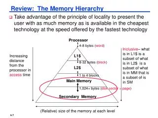
Introduction • The principle of locality says that most programs do not access all code or data uniformly • This principle plus the concept that smaller HW can be made faster, led to the design of hierarchies based memories • Figure 5.1shows a multi-level memory hierarchy, including typical sizes and speed of access • Memory hierarchy has increased with advances in performance of processors • Figure 5.2 plots processor performance against memory access • An architect should try to reduce the processor-memory speed gap! Dr. Anilkumar K.G
Introduction Dr. Anilkumar K.G
Introduction Dr. Anilkumar K.G
Introduction – Cache(1) • Cache is the name given to the highest or first level of memory hierarchy (Figure C.1 shows hierarchy levels) • Taking advantage of principle of locality • Temporal locality tells the likelihood of a used word (instruction) in the near future, so it is in the cache and can be accessed quickly • Spatial locality tells the high probability of next needed word (instruction) is in the block • Cache hit: when the processor finds a requested data item in the cache • Cache miss: when the processor does not find the needed data item in the cache • Blockor line: A fixed-size collection of data containing the requested word Dr. Anilkumar K.G ( SC6231)
Introduction – Cache (2) • The time required for a cache missdepends on both the latency and BW(bandwidth) of the memory • Latency determines the time to retrieve the first word of a memory block • BW determines the time to retrieve the rest of this block • A cache miss is handled by HW and causes CPU using in-order execution to pause or stall until the data are available • Not all objects referenced by a program need to reside in MM (Main Memory) • For program objects virtual memory (VM) can be referenced Dr. Anilkumar K.G ( SC6231)
Memory Hierarchy Dr. Anilkumar K.G ( SC6231)
Cache Performance Review (1) • One method to evaluate cache performance is to expand processor execution time with memory stall cycles, • the no. of cycles during which the processor is stalled (waiting for memory access is memory stall cycles) CPU time= (CPU clock cycles + Memory stall cycles) x Clock cycle time (1) CPU time = (IC x CPI + Mem. stall cycles/Instruction) x clock cycle time (2) • The equation (2) assumes that the CPU clock cycles include time to handle a cache hit, and the processor is stalled during a cache miss Dr. Anilkumar K.G ( SC6231)
Cache Performance Review (2) • The no. of memory stall cycles depends on both the no. of cache misses and cachemiss penalty: Memory stall cycles = No. of misses/instruction x Miss penalty(3) No. of misses = IC x (Misses/ Instruction) (4) Misses/Instruction = (Memoryaccesses/Instruction) x Miss rate (5) By applying (5) into (4) No. of misses = IC x (Memoryaccesses/Instruction) x Miss rate (6) Applying (6) into (3) Memory stallcycles = IC x (Memoryaccesses/Instruction) x Miss rate X Miss penalty(7) • The component, miss rate is the fraction of cache accesses that result in a miss • Now a days all processors provide HW to count the no. of misses and memory references Dr. Anilkumar K.G ( SC6231)
Cache Performance Review (3) • The Equation (7) is just an approximation since miss rate and miss penalty are different for cache reads and writes • Memory stall clock cycles can be given in terms of cache reads and writes: Memory stall cycles = IC x Reads/instruction x Read miss rate x Read miss penalty + IC x Writes/instruction x Write miss rate X Write miss penalty(8) • Simplify Eq (8) by combining reads and writes and finding the average miss rates and miss penalty for reads and writes (same as the Eq (7)): Memory stall cycles = IC x Memory accesses/Instruction x Miss rate x Miss penalty • The miss rate is one of the most important measures of cache design Dr. Anilkumar K.G ( SC6231)
Cache Performance Review (4) • Example: Assume that a computer has CPI is 1.0 when all memory accesses hit in the cache. The only data accesses are loads and stores, and these total 50% of the instructions (that is, 50% of instructions are load/store and one instruction access includes 0.5 data access). If the miss penalty is25 clock cycles and the miss rate is 2%, how much faster would the computer be if all instructions were cache hits? Dr. Anilkumar K.G ( SC6231)
First, need to compute the hit performance (apply Eq. (2)) CPU timehit = (IC x CPI + Mem.stall cycles/Instruction) x clock cycle time = (IC x 1 + 0 )x Clock cycle time {hit never cause a stall = IC X Clock cycle time (a) • Compute with cache, first compute memory stall cycles (apply Eq.(7)) Memory stall cycles = IC x( Mem.accesses /Instruction) x miss rate x miss penalty = IC x (1 + 0.5) x 0.02 x 25 = IC x 0.75 (b) { (1 + 0.5) represents one instruction access from Mem and each instruction with 0.5 data accesses} • Second, compute CPU exe. time with cache access (with mem.stall) CPU timecache-access = (IC x 1 + IC x 0.75) x clock cycle time ; where (IC x 0.75) is the memory stall cycles from (b) = 1.75 x IC x Clock cycle time Performance ratio: CPU timecache-access / CPU timehit = 1.75 i.e,computer with no cache misses (only hits) is 1.75 times faster Dr. Anilkumar K.G ( SC6231)
Cache Performance Review (5) • Some designers prefer miss rate as misses per instruction rather than misses per memory reference • These two are related (from (5)) Misses/instruction = (memory access/instruction)x miss rate • (Misses/Instruction) are often reported as (misses/1000 instructions) to show integers instead of fractions • The advantage of misses per instructionis that it is independent of the HW implementations • The drawback is that misses per instructionis architecture dependent; for e.g., the average no. of memory accesses per instruction vary with Intelx86 to MIPS processors Dr. Anilkumar K.G ( SC6231)
Misses per 1000 instructions • Designers prefer measuring miss rateas misses per instruction rather than misses per memory reference Misses = miss rate x memory accesses from(5) InstructionInstruction count (IC) = miss rate x memory accesses IC Dr. Anilkumar K.G ( SC6231)
Cache miss rate calculation from misses per 1000 instructions Misses/1000 instruction = miss rate x memory accesses 1000 Instruction (IC) Miss rate = misses/1000 instruction 1000 (9) Memory accesses Instruction (IC) Dr. Anilkumar K.G ( SC6231)
Cache miss rate calculation from misses per 1000 instructions • To show the equivalency between the two miss rate equations; a miss rate per 1000 instruction is 30. What is the memory stall time in terms of instruction count (IC)? Assume that miss penalty is 25 clocks. Memory stall clock cycles = IC x Memory accesses/Instruction x Miss rate x Miss penalty Apply Eq(9) for Miss rate = IC x (memory accesses/Instruction) x (misses/1000 instructions / 1000/memory access/instruction) x miss penalty = (IC x 30 x 25)/1000 = (IC x 750)/1000 = IC x 0.75 Dr. Anilkumar K.G ( SC6231)
Four Memory Hierarchy Questions • Where can a memory block be placed in the cache? • Block placement issue • How is a memory block found if it is in the cache? • Block identification issue • Which memory block should be replaced on a miss? • Block replacement issue • What happens on a write? • Write strategy issue Dr. Anilkumar K.G ( SC6231)
Block Placement (1) • Figure C.2 shows the restriction on where a block is placed, create 3 categories of cache organization • If each block has only one place it can appear in the cache, the cache is said to be direct mapped and the mapping: (Block address) MOD (Number of blocks in cache) • i = j mod C, where i is the cache line number assigned to j main memory blocks (total blocks) and C (mod value correlated to cache line) • for example, j = 64, C = 4: • Line 0 can hold blocks 0, 4, 8, 12, ..., 60 • Line 1 can hold blocks 1, 5, 9, 13, ..., 61 • Line 2 can hold blocks 2, 6, 10, 14, ...,62 • Line 3 can hold blocks 3, 7, 11, 15, ...,63 Dr. Anilkumar K.G ( SC6231)
Block Placement(2) • If a block can be placed anywhere in the cache, the cache is said to be fully associative • If a block can be placed in a restricted set of places in the cache, the cache is set associative • A set is a group of blocks in the cache • A block is first mapped onto a set and then the block can be placed anywhere within that set • If there are n blocks in a set, the cache is n-way set associative Dr. Anilkumar K.G ( SC6231)
Block Placement (3) • Direct mapped is simply one-way set associative cache • A fully associative cache with m blocks is called “m-way set associative” • The vast majority of caches today are directed mapped, two-way or four-way set-associative Dr. Anilkumar K.G ( SC6231)
Block Identification (1) • Caches have an address tag on each block frame that gives the block address • The tag of every cache block might contain the desired information is checked to see if it matches the block address from the CPU • All possible tags are searched in parallel • There must be a way to know that a cache block does not have valid information ( a valid bit is attached along with the tag) • If the valid bit is not set, then there is no address match allowed Dr. Anilkumar K.G ( SC6231)
Block Identification (2) • Processor address to the cache: • Figure C.3 shows how an address is divided for accessing a cache • The first division is between block address and the block offset • the block frame address can be further divided into tag field and index field • The block offset field selects the desired data from the block, • the index field selects the set, and • the tag field is compared against it for a hit Dr. Anilkumar K.G ( SC6231)
Block Identification (3) • Increasing the associativity increases the no. of blocks per set • Thereby decreasing the size of the index and increasing the size of the tag Dr. Anilkumar K.G ( SC6231)
Exercise • Consider a 8MB cache (assume that there is no level 2 cache in the system) and a 4GB main memory. If the size of a main memory block is 128-bit (eight, 16-bit words), then show the address fields which are used by a processor to access the following cache organizations; Direct map Fully associative map 2-way set associative map Dr. Anilkumar K.G ( SC6231)
Block Replacement (1) • When a miss occurs, the cache controller must select a block to be replaced with the a block that contains the desired data • In direct-mapped organization, the placement decision is made by HW only and hence no separate block replacement algorithm is needed • Only one block is checked for a hit and only that block can be replaced • With fully associative or set associative placement, there are many blocks to choose from a miss • There are three strategies employed for selecting a block for replacement are: Dr. Anilkumar K.G ( SC6231)
Block Replacement (2) • Random – blocks are randomly selected for replacement • It is simple build in HW • Least-recently used (LRU) – to reduce the chance of throwing out information that will be needed soon, accesses to blocks are recorded • The block replaced is the one that has been unused for the longest time • Expensive to implement • First-in-first out (FIFO) – because LRU can be complicated to calculate, FIFO approximates LRU by finding the older blocks Dr. Anilkumar K.G ( SC6231)
Write Strategy (1) • Reads dominates processor-cache accesses • All instruction fetches are reads and most instructions don’t write to memory • The block can be read from cache at the same time that the tag is compared • So the block read begins as soon as the block address is available • If the read is a hit, the requested data from the block is passed to CPU, else no benefit and results a miss consequences • Such optimism is not allowed for writes • Modifying a block cannot begin until the tag is checked to see if the address is a hit • During a write, tag checking cannot occur in parallel and writes take longer than reads Dr. Anilkumar K.G ( SC6231)
Write Strategy (2) • Another complexity in write is that the processor specifies the size of the write • Usually 1 to 8 bytes and only that portion of a block can be changed • Read can accesses more bytes • There are two write policies • Write through – the information is written to both the block in the cache and to the block in the main memory • Write back – the information is written only to the block in the cache • The modified block is written to main memory only when it is replaced Dr. Anilkumar K.G ( SC6231)
Write Strategy (3) • To reduce the frequency of writing back blocks on replacement, a dirty-bit is used • This status bit indicates whether the block is dirty (modified in the cache)or clean (not modified) • If the block is clean, the block is not written back on a miss • Both write back and write through have their advantages: • With write back, writes occurs at the speed of the cache and multiple writes within a blockrequire only on write to the lower-level memory • With write back, writes do not go to main memory hence uses less memory BW • Good for multiprocessors and embedded applications Dr. Anilkumar K.G ( SC6231)
Write strategy (4) • With write through • Copy of cache block available in lower level, which simplifies data coherency (write happens both cache and main memory simultaneously – in the same clock cycles) • easier to implement • The cache is always clean • Read misses never result in writes to the lower level (MM) • Data coherency is important for multiprocessors • When the processor must wait for writes to complete during a write through, is a write stall • A write buffer reduces write stalls, allow the processor to write to the buffer before the block is ready • Write stalls can occur even with write buffers Dr. Anilkumar K.G ( SC6231)
Write strategy (5) • There are two options on a write miss (block which is to be written is missing): • Write allocate– the block is allocated on a write miss • Write misses act like read misses • Blocks that are written will still be in the cache with write allocate • No-write allocate – write misses do not affect the cache, instead the block is modified only in the lower-memory (MM) • Thus blocks stay out of the cache in no-write allocate until the program tries to read the blocks Dr. Anilkumar K.G ( SC6231)
Write strategy (6) • Normally write back caches use write-allocate • Hoping that subsequent writes to that block will be captured by the cache • Write through caches often use no-write allocate • Even if there are subsequent writes to that block, the writes must still go to the lower-level memory Dr. Anilkumar K.G ( SC6231)
Instruction and Data Caches • Figure C.6 shows that instruction caches have lower miss rates than data caches • Separating instructions and data removes misses due to conflicts between instruction blocks and data blocks • Calculating the average miss rate with separate instruction and data caches necessitates knowing the percentage of memory references to each cache (data and instruction) • About 74% instruction references and about 26% data references (from Figure B.27) Dr. Anilkumar K.G ( SC6231)
Cache Performance • Because of the IC (instruction count) is independent of the HW, it is tempting to evaluate processor using that value • Similarly, evaluating memory hierarchy performance is to concentrate on miss rate, it is independent of the HW as well • A better measure of memory hierarchy performance is the Average Memory Access Time(AMAT) AMAT = Hit time + Miss rate x Miss penalty (10) • AMAT can be measured in absolute time: 0.25 to 1 ns on a hit, or 150 to 200 clock cycles on a miss • AMAT is an indirect measure of performance; it is better than miss rate but it is not a substitute for execution time Dr. Anilkumar K.G ( SC6231)
Cache Performance - Example • Assume that the hit time of a 2-way set-associative L1 data cache is 1.2 times faster than a 4-way set-associative cache of the same size. The miss rate of 2-way cache is 0.049 and 4-way is 0.044 (for an 8KB data cache). Assume a hit is 1 clock cycle. Assume the miss penalty is 11 clock cycles for the 2-way set-associative cache, and the miss penalty of 4-way is 2 clocks less than 2-way cache. Calculate their AMATs (Average Memory Access Time). Dr. Anilkumar K.G ( SC6231)
AMAT and Processor Performance(1) • Designers are often assume that all memory stalls are due to cache misses • The processor stalls during misses, and the memory stall time is strongly correlated to AMAT • Consider the CPU time (exe. Time): CPU time = (CPU clock cycle + Mem. Stall clock cycles)x Clock cycle time CPU time = IC x(CPI + Mem.Stall clocks/Instruction) x Clock cycle time • This formula raises the question of whether the clock cycles for a cache hit should be considered part of CPU execution clock cycles or part of memory stall clock cycles Dr. Anilkumar K.G ( SC6231)
AMAT and Processor Performance(4) • Cache misses have a double-barreled impact on a processor with a low CPIand a fast clock: • Lower the CPI, the higher the relative impact of a fixed no. of cache miss clock cycles • When calculating CPI, the cache miss penalty is measured in processor clock cycles for a miss • Even if memory hierarchies for two computers are identical, the processor with the higher clock rate has a larger no. of clock cycles/miss and hence a higher memory portion of CPI • Minimizing the AMAT is a reasonable goal – the final goal is to reduce CPU time (exe. time) Dr. Anilkumar K.G ( SC6231)
Basic Cache Optimizations(1) • The AMAT formula provide a framework to present cache optimizations for improving performance: AMAT = Hit time + Miss rate x Miss penalty • Hence organize cache organizations into three categories (Figure C.17 shows summary): • Reducing the miss rate: larger block size, larger cache size and higher associativity • Reducing the miss penalty: multi-level caches and giving reads priority over writes • Reducing the time to hit in the cache: avoiding address translation when indexing the cache Dr. Anilkumar K.G ( SC6231)
Basic Cache Optimizations(2) • A model that sort all cache misses into 3Cs: • Compulsory (C1)– the every access to a block cannot be in the cache, so the block must be brought into the cache • Also called cold-start misses or first-reference misses • Capacity(C2)– if the cache cannot contain all the blocks needed during execution of a program, capacity misses (in addition to compulsory misses) will occur • Because of blocks being discarded and later retrieved • Conflict (C3) – if the block placement strategy is set associative or direct mapped, conflict misses will occur • Because a block may be discarded and later retrieved if too many blocks map to its sets. These misses are called collision misses Dr. Anilkumar K.G ( SC6231)
Designer’s Solution for 3Cs • Fully associative placement avoids all conflict misses • Fully associativity is expensive in HW, may slow the processor clock, leading overall low performance • To make blocks larger to reduce the number of compulsory misses • But large blocks can increase other kinds of misses • Changing cache size changes conflict misses as well as capacity misses • A larger cache spreads out references to more blocks • Thus a miss might from capacity miss to a conflict miss changes Dr. Anilkumar K.G ( SC6231)
First Optimization: Larger Blocks to Reduce Miss Rate • The simplest way to reduce miss rate is to increase the block size • Figures C.10 & C.11 the trade-off of block size vs. miss rate and cache sizes • Larger block sizes will also reduce compulsory misses • Because of the principle of locality: larger blocks take advantage ofspatial locality – Larger blocks have more words • At the same time larger blocks increase the miss penalty • Larger blocks reduce the no. of blocks in the cache, they may increase conflict misses and capacity misses if the cache is small • Larger blocks increase miss penalty (Figure C.12) Dr. Anilkumar K.G ( SC6231)
First Optimization: Larger Blocks to Reduce Miss Rate Dr. Anilkumar K.G ( SC6231)
First Optimization: Larger Blocks to Reduce Miss Rate Dr. Anilkumar K.G ( SC6231)