Download
1 / 37
370 likes | 477 Vues
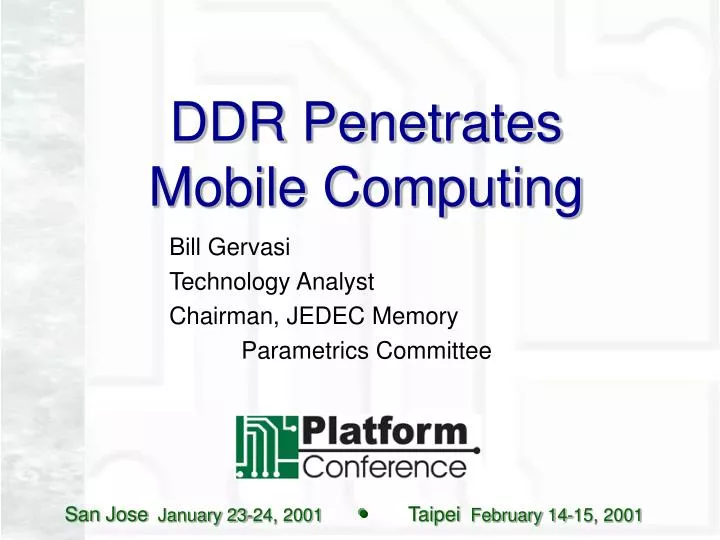
DDR Penetrates Mobile Computing. Bill Gervasi Technology Analyst Chairman, JEDEC Memory Parametrics Committee. Agenda. Why DDR for Mobile? Standard versus cached DRAMs DDR Configurations Introducing the DDR MicroDIMM Mobile System Design Guidelines. Reasons for DDR in Mobile.

E N D
DDR PenetratesMobile Computing Bill Gervasi Technology Analyst Chairman, JEDEC Memory Parametrics Committee
Agenda • Why DDR for Mobile? • Standard versus cached DRAMs • DDR Configurations • Introducing the DDR MicroDIMM • Mobile System Design Guidelines
Reasons for DDR in Mobile • Performance • Power • Form factors
SDR SDRAM Evolution 4800MB/s DDR II MainstreamMemories 2700MB/s DDR333 2100MB/s DDR266 Simple,incrementalsteps 1000MB/s
Power: DDR vs SDR DDR-266 3.2X DDR-333 2.6X est. PC-100 1X PC-133 0.8X
RelativePower CPU ClockLatency** Active on PowerState* 100% 4% 12% 0 x 5 = 0 Inactive on 3 x 5 = 15 Active off 1 x 5 = 5 Inactive off 0.2% 4 x 5 = 20 * Not industry standard terms – simplified for brevity ** Assuming memory clock frequency = 1/5 CPU frequency ClosedPage Sleep OpenPage 0.4% 200 x 5=1000 DDR Power Management
Implications: Mobile Power • Encourages closed page policy • Precharge banks as soon as data read • Takes latency hit to reactivate
Closed Page Power Profile Higher Power Power Profile NOP ACT R R PRE NOP Command Activity Power Profile NOP ACT W W PRE NOP Command Activity Lower Power
Cached DRAM Power Profile Higher Power Power Profile NOP ACT R-PRE R R NOP Command Activity Depending on cached DRAM architecture Power Profile NOP ACT W W PRE NOP Command Activity Lower Power
Standard vs Cached • Cached DRAM architectures save power • Improved closed page performance • Latency reduction on page hits • Lower power profile (See my other presentation at Platform 2001… “An Analysis of Virtual Channel and Enhanced Memories Technologies”)
DDR Configurations TSOP-II DIMM NEW! FBGA TQFP SO-DIMM NEW! MicroDIMM
Next: Small Packages FBGA(fine pitch BGA) • Lower inductance • Lower capacitance • Smaller footprint • Tighter layouts enabled Details: Package size = 104 mm2 = 54% smaller Inductance: 1.7nH lower Inductance variation, pin to pin: 3X less Capacitance: 0.5pF lower Performance gain: 300ps of data valid time
DDR Chip Configurations • TQFP devices for point to point • x32 … 64Mb, 128Mb coming • 100 pins, 16 x 22 mm footprint • TSOP devices • x4, x8, x16 … 64Mb, 128Mb, 256Mb • 66 pins, 12 x 22 mm footprint • FBGA selection in process • x4, x8, x16 … 128Mb, 256Mb, 512Mb/1Gb coming • 60 ball, 6.4 x 11 mm minimum footprint
DDR Module Configurations • DDR SO-DIMM – done! • Sockets, modules in production • DDR MicroDIMM – in process • Task group active • System application combinations • One module only • Soldered down + module • Two modules
Next: DDR MicroDIMM • Half the size of the DDR SO-DIMM • Half the capacity if using TSOP – or – • Same capacity if using FBGA • Target markets: • PDAs • Internet appliances • Subnotebook computers
SO- and Micro- DIMMs DDR SO-DIMM TSOP:67.6 x 31.75 mm = 2146 mm2 4 or 8 devices 200 pins on 0.6 mm pin pitch(supports ECC) --------------------- FBGA:Under consideration if needed DDR MicroDIMM TSOP:45.5 x 30 mm = 1365 mm2 4 devices 172 pins on 0.5 mm pin pitch(no ECC) --------------------- FBGA:45.5 x 25 mm = 1137 mm2 4 or 8 devices
Module Status • DDR SO-DIMM • DDR266 validated • DDR333 under analysis • Looking okay to 333 MHz with TSOP • DDR MicroDIMM • TSOP easy, DDR266/333 speeds • FBGA package needed to fit 8 chips • Possible schedule • Sample April 2001 • Approved spec June 2001
Small System Configurations • One data bus, one address bus • Point to point, single socket • Series damped data, address, clock • Two sockets • SSTL_2 terminated data • Series damped address, clock • Top/bottom or butterfly arrangement
Top/Bottom Mobile Modules Motherboard • Standard for many current full size notebooks • Hard to get at one of the modules • Thickest form factor Module SOCKET CPU CPU Socket Module Note: There may be patents regarding use of these layouts
Butterfly Mobile Modules Module SOCKET CPU Motherboard • Perfect for thin/light notebooks & subnotes • Single access door to both modules • Also good for small form factor desktop PCs -- or -- CPU Module Socket Note: There may be patents regarding use of these layouts
MicroDIMM Designs You know the DDR SO-DIMM, so… …let’s focus on the MicroDIMM design First, system configurations…
RAM Conn RAM 25 25 RAM RAM Clock Topology CK CK
RAM RAM 25 22 Data Topology, 1 Slot DQ, DQS, DM 2 bank Conn
RAM RAM Conn RAM RAM 25 22 22 25 Data Topology, 2 Slot DQ, DQS, DM 2 bank VTT Conn 2 bank
RAM RAM RAM RAM RAM RAM RAM RAM 10 A/C Topology, 1 Slot Two Bank MicroDIMM shown Conn A, BA, WE, RAS, CAS
RAM RAM RAM RAM Conn 10 A/C Topology, 1 Slot One Bank MicroDIMM shown A, BA, WE, RAS, CAS 11pF
RAM RAM RAM RAM RAM RAM RAM RAM RAM RAM RAM RAM Conn 10 A/C Topology, 2 Slot Two Bank MicroDIMM shown One Bank MicroDIMM shown Conn A, BA, WE, RAS, CAS 11pF
RAM RAM RAM RAM Conn 10 CS & CKE Topology One or Two Bank MicroDIMM shown CS, CKE 11pF
Increasing Focus on Systems • JEDEC packaging committee charter extended to include module sockets • Land pattern for pin pads • Mechanical support tab locations • Orientation holes • Shadow area of socket body • Module height & centerline • Working system configuration first time!
DDR MicroDIMM Clearances 3.78mm max 4.43mm max discretes Standard socket, double sided memory module Standard socket, single sided memory module 3.78mm max 5.40mm max 0.65mm min Reverse socket, double sided memory module Reverse socket, single sided memory module
Socket Spec Status • Merging 144, 172 pin sockets into single parameterized MO-214 spec • Priming spring included • Shoves module “to the left” • Redimensioned by left edge, not center • Edge bevel defined
Conclusions • DDR solutions for mobile growing • Cached DRAM would be even better • Point to point and DDR SO-DIMM done • DDR333 development in progress • FBGA packaged DDR coming • DDR MicroDIMM development on track
DDR Memory of choice for the future