Download

1 / 14
140 likes | 156 Vues
Learn about the key functional units needed to construct a datapath, including registers and memory, for efficient data processing in a lab setting. Understand how to utilize a 32-bit MIPS register file for data storage and manipulation.

E N D
Datapath Components for Lab The Processor! (4.1- 4.4 4th ed)
Review: How Registers work Write Enable Data In Data Out • Register • Similar to D Flip Flop • N-bit input and output • Write Enable input • Write Enable: • negated (0): Data Out will not change • asserted (1): Data Out will become Data In after clock edge N N Clk
MIPS Register File RW R1 R2 5 5 5 Write Enable Read data 1 Write data 32 32 32-bit Registers • Register File consists of 32 registers: • Two 32-bit output busses: Read data 1 & Read data 2 • A 32-bit input bus: write data • Register is selected by: • R1(read register 1) selects the register to put on read data 1 • R2(read register 2) selects the register to put on read data 2 • RW(write register) selects the register to be writtenvia (write data) when Write Enable is 1 (Regwrite) • Clock input (CLK) • The CLK input is a factor ONLY during write operation • During read operation, behaves as a combinational logic block: • Read data1 & read data 2 valid after “access time.” 32 Read data 2 Clk 32
Memory Write Enable Address Write data read data Data In DataOut 32 32 • Memory (Data) • input bus: Data In (Write data) • output bus: Data Out (Read Data) • Memory word selected by: • Address selects word to put on Data Out • Write Enable = 1: address selects memoryword to be written via the Data In bus (Memwrite) • Clock input (CLK) (omitted from Book diag for simplicity) • The CLK input is a factor ONLY during write operation • During read operation, behaves as a combinational logic block: • Address valid => Data Out valid after “access time.” • Instruction memory data not shown in Book for simplicity Clk
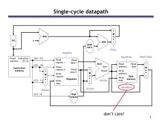
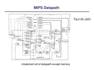
M A d d u x A L U 4 A d d r e s u l t S h i f t t 2 l e f R e g i s t e r s R e a d R e a d r e g i s t e r 1 P C R e a d a d d r e s s R e a d d a t a 1 Z e r o r e g i s t e r 2 A L U I n s t r u c t i o n A L U R e a d A d d r e s s W r i t e R e a d r e s u l t M d a t a r e g i s t e r M d a t a 2 u I n s t r u c t i o n u x W r i t e D a t a x m e m o r y d a t a m e m o r y W r i t e d a t a 3 2 1 6 S i g n e x t e n d Complete Single Cycle Datapath for : R, LD/ST, BEQ Can execute basic instructions in a single clock cycle No resource can be used more than one time during a single cycle
Requirements: CPU needs a 32-bit ALU (1) Functional Specification inputs: 2 x 32-bit operands A, B, 4-bit mode outputs: 32-bit result S, 1-bit carry, 1 bit overflow operations: add, addu, sub, subu, and, or, xor, nor, slt, sltU (2) Block Diagram (schematic symbol/ Verilog description) 32 32 A B 4 ALU c m ovf S 32
sum Cin A B 1-bit adder Review (Appendix B.5, B.6) Cin a Sum 1unit of delay from Cin to sum b Co 2 units of delay from A/B to sum Sum = a!bc! + ab!c! + a!b!c+abc = a b c = XOR Carryout = a!bc + ab!c + abc! + abc
Carry Out circuit Cin a b 2 units of delay from Cin to Cout Cout
Additional operations: Subtract, AND, OR S-select invert CarryIn • A - B = A + (– B) = A + B + 1 • form two complement by invert and add one and A or Result Mux add 1-bit Full Adder B CarryOut
Binvert Operation CarryIn a 0 1 Result b 0 2 1 Less 3 a. CarryOut Binvert Operation CarryIn a 0 1 Result b 0 2 1 Less 3 Set Overflow Overflow detection b. 1-bit ALU: AND, OR, a+b, a+b! ALU Delays Result = 1 gate delay From a to result = 2 Form b to Result = 2 (ignore b invert) Most significant bit
Cin operation 32-bit ALU using ripple carry adder a0 Sum0 ALU0 b0 a1 Sum1 ALU1 b1 Sum2 ALU2 a31 Sum31 b31 ALU31
Bnegate a0 Result0 b0 ALU0 Less CarryOut Result1 a1 CarryIn b1 ALU1 0 Less Zero CarryOut Result2 a2 CarryIn b2 ALU2 0 Less CarryOut Result31 a31 CarryIn Set b31 ALU31 Overflow 0 Less Operation Final 32-bit ALU, including zero detect