Download
1 / 114
2.43k likes | 4.32k Vues
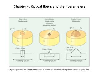
Chapter 4 - Optical sensors:. Optical sensors. Optical sensors are those sensors that detect electromagnetic radiation in the broad optical range – from far infrared to ultraviolet

E N D
Optical sensors • Optical sensors are those sensors that detect electromagnetic radiation in the broad optical range – from far infrared to ultraviolet • Approximate range of wavelengths from 1mm (3x10¹¹ Hz or far infrared) to 1 nm (3x10¹⁷ Hz or upper range of the ultraviolet range). • Direct methods of transduction from light to electrical quantities (photovoltaic or photoconducting sensors) • Indirect methods such as conversion first into temperature variation and then into electrical quantities (PIR sensors).
Spectrum of “optical” radiation • Nomenclature: • Visible light • Infrared radiation (not infrared “light”) • Ultraviolet radiation (not UV “light”) • Ranges shown are approximate and somewhat arbitrary
Infrared radiation • Approximate spectrum • 1mm (300 GHz) to 700nm (430 THz) • Meaning: below red • Near infrared (closer to visible light) • Far infrared (closer to microwaves) • Invisible radiation, usually understood as “thermal” radiation • 1nm=10-9m 1GHz=109 Hz, 1THz=1015 Hz
Visible light • Approximate spectrum • 700nm (430 THz) to 400nm (750 THz) • Based on our eye’s response • From red (low frequency, long wavelength) • To violet (high frequency, short wavelength) • Our eye is most sensitive in the middle (green to yellow) • Optical sensors may cover the whole range, may extend beyond it or may be narrower
Ultraviolet (UV) radiation • Approximate spectrum • 400nm (750 THz) to 400pm (300 PHz) • Meaning - above violet • Understood as “penetrating” radiation • Only the lower end of the UV spectrum is usually sensed • Exceptions: radiation sensors based on ionization (chapter 9)
A word on units • SI units include: meter, kg, second, ampere, candela, temperature kelvin and the mole • All other units are derived units • Candela “is the luminous intensity, in a given direction, of a source that emits monochromatic radiation of frequency 540x1012 Hz and that has a radiation intensity of 1/683 watt per steradian”
Optical sensing • Based on two principles • Thermal effects of radiation • Quantum effects of radiation • Thermal effects: absorption of radiation of the medium through increased motion in atoms. This may release electrons (heating) • Quantum effects: photon interaction with the atoms and the resulting effects, including release of electrons.
The photoelectric effect • Planck’s equation: e=hf [ev] h = 6.6262x10 [joule.second] (Planck’s constant) f = frequency e = energy of a photon at radiation frequency f. • This is called the quantum of energy • Higher for higher frequency • Can be imparted to electrons as kinetic energy Note: this energy is also called ionization energy and is used to distinguish between “dangerous” and “benign” radiation
The photoelectric effect • Photons collide with electrons at the surface of a material • The electrons acquire energy and this energy allows the electron to: • Release themtselves from the surface of the material by overcoming the work function of the substance. • Excess energy imparts the electrons kinetic energy.
The photoelectric effect • This theory was first postulated by Einstein in his photon theory (photoelectric effect) in 1905 (for which he received the Nobel Prize): hf - e0 = k e0 is called the work function (energy required to leave the surface of the material) k represents the maximum kinetic energy the electron may have outside the material. Energy is “quantized”
The photoelectric effect • For electrons to be released, the photon energy must be higher than the work function of the material. • Frequency must be sufficiently high or: • Work function must be low • Frequency at which the photon energy equals the work function is called a cutoff frequency • Below it no quantum effects may be observed (only thermal effects) • Above it, thermal and quantum effects are present. • At higher frequencies (UV radiation) quantum effects dominate.
Some notes: • Thermoelectric effect is a surface effect • Most notable in conductors • Group 1 (Alkalis) has lowest work function values - often used in thermoelectric cells (later) • The amount of electrons released becomes a measure of radiation intensity • Electrons may be emitted by thermionic emission - a totally different issue based on thermal effect
The photoconducting effect • A solid state (volume) effect • Most notable in semiconductors • Based on displacement of valence and/or covalence electrons • Valence electrons: bound to individual atoms in outer layers • Covalence electrons: bound but shared between neighboring atoms in the crystal
Model: photoconducting effect • Photons collide with electrons • Electrons must acquire sufficient energy to: • Leave the valence band • Move into the conduction band • Minimum energy required: band gap energy
Model: photoconducting effect • In the conduction band, electrons are mobile and free to move as a current. • When electrons leave their sites, they leave behind a “hole” which is simply a positive charge carrier. • This hole may be taken by a neighboring electron with little additional energy (recombination) • Net current is due to electrons and holes. • Manifested as a change in concentration of carriers (electrons and holes) in the conduction band and therefore in conductivity of the medium
Model: photoconducting effect • Conductivity of the medium is: • e - charge of electron • e - mobility of electrons [m2/Vs] • p - mobility of holes [m2/Vs] • n - concentration (density) of electrons [/m3] • p - concentration (density) of holes [/m3] • s - conductivity of the medium • Conductivity is temperature dependent (mobility and concentrations are temperature dependent)
photoconducting effect • This change in conductivity or the resulting change in current is the a direct measure of radiation intensity. • The photoconducting effect is most common in semiconductors because the band gaps are relatively small. • It exists in insulators as well but there the band gaps are very high and therefore it is difficult to release electrons except at very high energies. • In conductors, most electrons are free to move (they are in the conduction band and hence far above the band gap in energy) which indicates that photons will have minimal or no effect on the conductivity of the medium. • Semiconductors are the obvious choice for sensors based on the photoconducting effect while conductors will most often be used in sensors based on the photoelectric effect
Photoconducting effect • Conductivity results from the charge, mobilities of electrons and holes and the concentrations of electrons, n and p from whatever source. • In the absence of light, the material exhibits what is called dark conductivity, which in turn results in a dark current. • Depending on construction and materials, the resistance of the device may be very high (a few MegaOhms (M) or a few k. • When the sensor is illuminated, its conductivity changes depending on the change in carrier concentrations (excess carrier concentrations).
Photoconducting effect • This change in conductivity is • Carriers are generated at a certain generation rate • They also recombine at a recombination rate typical for the material, wavelength, carrier lifetime, etc. • Generation and recombination exist simultaneously • Under a given illumination a steady state is obtained when these are equal. • Under this condition, the change in conductivity is (tp,tn - lifetimes, f - # of carriers generated per second per volume
Photoconducting effect • If p - type carriers dominate - p-type photoconductor • If n - type carriers dominate - n type photoconductor • Opposite type carrier concentrations are negligible • A particular type is obtained by doping (see chapter 3)
Photoconducting effect - sensitivity • Sensitivity to radiation (efficiency) • L is the length of the sensor (distance between electrodes) and V the voltage across the sensor. • Sensitivity: the number of carriers generated per photon of the input radiation. • To increase sensitivity • materials with high carrier lifetimes • keep the length of the photoresistor small • the latter is typically achieved through the meander construction shown below
photoconducting effect • Properties vary among semiconductors • The lower the band gap the more effective the semiconductor will be at detection at low frequencies (long wavelengths). • The longest wavelength specified for the material is called the maximum useful wavelength, above which the effect is negligible. • Availability of electrons is temperature dependent - each semiconductor has a maximum useful temperature (see table)
Photoconductive properties • Example: InSb (Indium Antimony): • maximum wavelength of 5.5 m • sensitive in the near infrared range • band gap is very low - very sensitive. • but electrons can be easily released by thermal sources • totally useless for sensing at room temperatures (300K) (most electrons are in the conduction band) • These carriers serve as a thermal background noise for the photon generated carriers. • it is often necessary to cool these long wavelength sensors to make them useful by reducing the thermal noise.
Photodiodes • Semiconducting diode exposed to radiation • Excess carriers due to photons add to the existing charges in the conduction band exactly in the same fashion as for a pure semiconductor. • The diode itself may be reverse biased, forward biased or unbiased • Forward biased mode is not useful as a photosensor • Number of carrier in conducting mode is large • Number of carrier added by radiation small • Sensitivity is very low
Photodiode - two modes • Two modes of operation as photodiode • 1. Photoconductive mode • Diode is in reverse bias • Operates similarly to a photoconductor • 2. Photovoltaic mode • Diode is not biased • Operates as a source (solar cell for example)
Photoconducting mode • In dark mode there are very few carriers flowing • Photons release electrons from the valence band either on the p on n side of the junction. • These electrons and the resulting holes flow towards the respective polarities (electrons towards the positive pole, holes towards the negative pole) • A photocurrent, which in the absence of a current in the diode constitute the only current (a small leakage current exists - see equivalent circuit).
Photoconductive mode - additional effect • The large inverse bias accelerates the electrons • Electrons can collide with other electrons and release them across the band gap, • This is called an avalanche effect • it results in multiplication of the carriers available. • Sensors that operate in this mode are called photomultiplier sensors
Photoconductive mode - equivalent circuit • It is the total current in the load • Due to photons plus other sources • Thermal • Leakage • Capacitances, etc.
Photoconductive diode - operation • Current in reverse biased mode is: • I0 is the leakage current, • Vd is the voltage across the junction, • k=8.62x10⁻⁵ eV/K (Boltzman’s const.) • T is the absolute temperature • Current due to photons is: • P is the radiation power density (W/m2) • f is frequency • is called the quantum absorption efficiency • A is the area of the diode exposed (PA = power absorbed by the junction) • h is Planck’s constant
Photoconductive diode - operation (cont.) • Total external current is • I0 is typically small (negligible) • 10 nA or less • Neglecting I0, the total external current is • This current gives a direct reading of the power absorbed by the diode • It is not constant since the relation depends on frequency and the power absorbed itself is frequency dependent.
Photoconductive diode - operation (cont.) • As the input power increases the characteristic curve of the diode changes as shown, resulting in an increase in reverse current • This current represents the sensed quantity
Photodiode - construction • Any diode can serve as a photodiode if: • n region, p region or pn junction are exposed to radiation • Usually exposure is through a transparent window or a lens • Sometimes opaque materials are used (IR, UV) • Specific structures have been developed to improve one or more of the characteristics • The most important improvement is in the dark current
Photodiodes - construction • A - Oxide layer increases resistivity - reduced dark current • B. - PIN diode • Addition of the intrinsic p layer increases resistance • Reduces dark current • C. - pnn+ diode - a layer of conducting n+ added • Reduces resistance • Improves response to low wavelengths
Photodiodes - construction • D - A combination of B and C • Addition of the intrinsic p layer increases resistance • Reduces dark current and improves low wavelength response • E. - Schotky diode (metal-semiconductor junction) • Improved infrared (high wavelength) response • Metal layer (hold) must be transparent (very thin layer • F. - npp+ diode - as in B
Photodiodes - construction • Available in various packages and for various applications • Individual diodes in cans with lenses • Surface mount diodes used in infrared remote controls • Arrays (linear) of various sizes for scanners • Infrared and UV diodes for sensing and control
Photodiodes • Photodiode as used in Photodiode array used in a CD player a scanner
Photovoltaic diodes • The diode is not biased • Serves as a generator • Carriers generated by radiation create a potential difference across the junction • Any photodiode can operate in this mode • Solar cells are especially large-surface photodiodes
Photovoltaic mode • Equivalent circuit of photodiode in photovoltaic mode • Capacitance is usually large • Leakage current is small • Response of solar cells is slow due to very large capacitance