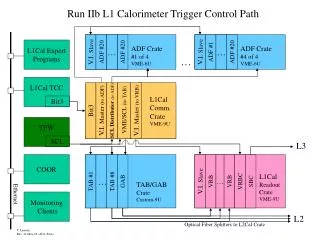
Download
1 / 17
170 likes | 247 Vues
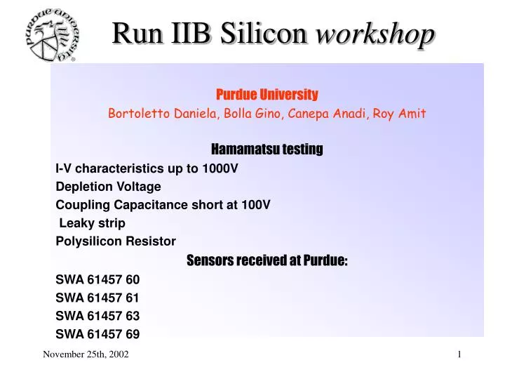
Run IIB Silicon workshop. Purdue University Bortoletto Daniela, Bolla Gino, Canepa Anadi, Roy Amit Hamamatsu testing I-V characteristics up to 1000V Depletion Voltage Coupling Capacitance short at 100V Leaky strip Polysilicon Resistor Sensors received at Purdue: SWA 61457 60

E N D
Run IIB Silicon workshop Purdue University Bortoletto Daniela, Bolla Gino, Canepa Anadi, Roy Amit Hamamatsu testing I-V characteristics up to 1000V Depletion Voltage Coupling Capacitance short at 100V Leaky strip Polysilicon Resistor Sensors received at Purdue: SWA 61457 60 SWA 61457 61 SWA 61457 63 SWA 61457 69
Run IIB Silicon workshop Purdue Testing results at www.physics.purdue.edu/cdf/RunIIB/pres sensor characterization I-V characteristics up to 1000V Depletion Voltage Coupling Capacitance & Oxide Leakage Current Polysilicon Resistor Interstrip Capacitance Radiation Hardness Test sensor SWA61457 60 sensor SWA61457 63 sensor SWA61457 69 have been irradiated at U.C.Davies facility fluence = 1.4 1014 1MeV eq-n cm-2 fully characterizated
Run IIB Siliconworkshop Sensor 60 I (120V) =62.6nA hamamatsu I(120V)=77.3nA Sensor 61 (bonding problems) I (V=150) =120nA hamamatsu I(150)=71 nA Sensor 63 I (V=140)=71nA hamamatsu I(140)=74.3nA Sensor 69 I (140V) =76.8nA hamamatsu I(140V)=81.3nA
Run IIB Siliconworkshop Neutron irradiation fluence 1.4 1014 1MeV n-eq cm^-2 Layer 0 Operating temperature T = -5C (TDR 3-16) Leakage current per strip module Istrip(V > Vd) 95 nA
Run IIB Siliconworkshop Annealing procedure on sensor 69 4min @ T=80C Both sensor 60 and sensor 69 I(plateau) 50uA (T = -25C) sensor 60:1400 min at T=20C sensor 69: 800 min at T = 20C & annealing Before Irradiation breakdown voltage =181V Assuming a=410-17 A/cm DI(Vdep) 7mA Measured value DI(Vdep) 5.5mA Estimated Fluence = 1.1 1014 1MeV n-eq
Run IIB Siliconworkshop Sensor 60 Vdep=117 V hamamatsu Vdep=140V Sensor 61 Vdep=141 V hamamatsu Vdep=160V Sensor 63 Vdep=133 V hamamatsu Vdep=160V Sensor 69 Vdep=132 V hamamatsu Vdep=150V
Run IIB Siliconworkshop ROSE/TN/2000-10 Version 1/14.12/2000 Vd (20C)=Vd(T)*1.0526/[1+A·exp(T/t)] A=0.00936 t = 11.58 Vd(f)=Vd(1kHz)[1-D·log(f/1kHz)] D=0.11+/-0.009 After irradiation Sensor 60 T=-25C,f=1kHz Vdep=137 V T=20C,f=10kHz Vdep=128 V
Run IIB Siliconworkshop After irradiation Sensor 69 Vdep(T=20C,f=100kHz) =136 V Vdep(T=20C,f=10kHz) =119 V After irradiation & after annealing Sensor 69 to be understood
Run IIB Siliconworkshop Open in the metal ? Sensor 60 Coupling Capacitance CC(100Hz)= 134.43+/-0.48pF Sensor 63 Coupling Capacitance CC(100Hz)= 125.32+/-1.99pF Sensor 690 Coupling Capacitance CC(100Hz)= 126.49+/-0.97pF
Run IIB Siliconworkshop Sensor 60 Coupling Capacitance CC(100Hz)= 136.34+/-1.17pF Sensor 69 Coupling Capacitance CC(100Hz)= 134.47+/-5.34pF
Run IIB Siliconworkshop Trend to be understood ? Sensor 60 Interstrip Capacitance Ci(1MHz)= 3.46+/-1.68pF Sensor 63 Interstrip Capacitance Ci(1MHz)= 3.17+/-0.01pF Sensor 69 Interstrip Capacitance Ci(1MHz)= 3.53+/-0.18pF
Run IIB Siliconworkshop Sensor 63 Interstrip Capacitance Ci(1MHz)= 3.39+/-0.07pF Sensor 60 Interstrip Capacitance Ci(1MHz)= 3.43+/-0.08pF
Run IIB Siliconworkshop Before Irradiation Sensor 60 R=1.72 +/- 0.2 MOhm Sensor 63 R=1.84 +/- 0.8 Mohm drop to be understood charge up ? After Irradiation Sensor 63 R=1.64 +/- 0.04 MOhm Sensor 63 R=1.7 +/- 0.8 Mohm
Run IIB Siliconworkshop Before Irradiation R=1.86 MOhm After Irradiation R=1.71 MOhm
Run IIB Siliconworkshop Conclusions We have evaluated the performance of Axial Outer Layer The sensors fulfill the specifications: Leakage Current as Small as expected Bad channel Not found Capacitance Values as Expected Bias Resistor as Expected Full Dep Voltage after Irradiation as Expected NEED to be understood: 1)Before Irradiation, Bias Resistance drop : Charge up ? 2)After Irradiation, Interstrip Capacitance bump : related to Bias Resistor ? 3)After Irradiation & After annealing, Total Capacitance increase at V>Vdep