Download
1 / 35
370 likes | 566 Vues
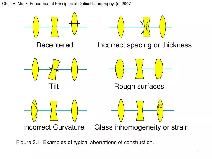
Figure 3.1 Examples of typical aberrations of construction. Figure 3.2 The reduction of spherical aberration by the use of a cemented doublet. . Figure 3.3 Example of a simple NA = 0.8, 248 nm lens design. (a). (b).

E N D
Chris A. Mack, Fundamental Principles of Optical Lithography, (c) 2007 Figure 3.1 Examples of typical aberrations of construction.
Chris A. Mack, Fundamental Principles of Optical Lithography, (c) 2007 Figure 3.2 The reduction of spherical aberration by the use of a cemented doublet.
Chris A. Mack, Fundamental Principles of Optical Lithography, (c) 2007 Figure 3.3 Example of a simple NA = 0.8, 248 nm lens design.
Chris A. Mack, Fundamental Principles of Optical Lithography, (c) 2007 (a) (b) Figure 3.4 Ray tracing shows that (a) for an ideal lens, light coming from the object point will converge to the ideal image point for all angles, while (b) for a real lens, the rays do not converge to the ideal image point.
Chris A. Mack, Fundamental Principles of Optical Lithography, (c) 2007 (a) (b) Figure 3.5 Wavefronts showing the propagation of light for (a) for an ideal lens, and (b) for a lens with aberrations.
Chris A. Mack, Fundamental Principles of Optical Lithography, (c) 2007 Figure 3.6 Example plots of aberrations (phase error across the pupil).
Chris A. Mack, Fundamental Principles of Optical Lithography, (c) 2007 (a) (b) Figure 3.7 Diffraction patterns from (a) a small pitch, and (b) a larger pitch pattern of lines and spaces will result in light passing through a lens at different points in the pupil. Note also that y-oriented line/space features result in a diffraction pattern that samples the lens pupil only along the x-direction.
Chris A. Mack, Fundamental Principles of Optical Lithography, (c) 2007 (a) (b) Figure 3.8 Phase error across the diameter of a lens for several simple forms of aberrations: a) the odd aberrations of tilt and coma; and b) the even aberrations of defocus and spherical.
Chris A. Mack, Fundamental Principles of Optical Lithography, (c) 2007 Figure 3.9 The effect of coma on the pattern placement error of a pattern of equal lines and spaces (relative to the magnitude of the 3rd order x-coma Zernike coefficient Z6) is reduced by the averaging effect of partial coherence.
Chris A. Mack, Fundamental Principles of Optical Lithography, (c) 2007 Figure 3.10 The impact of coma on the difference in linewidth between the rightmost and leftmost lines of a five bar pattern (simulated for i-line, NA = 0.6, sigma = 0.5). Note that the y-oriented lines used here are most affected by x-coma. Feature sizes (350 nm, 400nm, and 450 nm) are expressed as k1 = linewidth *NA/l.
Chris A. Mack, Fundamental Principles of Optical Lithography, (c) 2007 Figure 3.11 Variation of the resist profile shape through focus in the presence of coma.
Chris A. Mack, Fundamental Principles of Optical Lithography, (c) 2007 (a) (b) Figure 3.12 Examples of isophotes (contours of constant intensity through focus and horizontal position) for a) no aberrations, and b) 100 ml of 3rd order coma. (NA = 0.85, l = 248nm, s = 0.5, 150 nm space on a 500 nm pitch).
Chris A. Mack, Fundamental Principles of Optical Lithography, (c) 2007 (a) (b) Figure 3.13 Chromatic aberrations: a) measurement of best focus as a function of center wavelength shows a linear relationship with slope 0.255 mm/pm for this 0.6 NA lens; b) degradation of the aerial image of a 180-nm line (500-nm pitch) with increasing illumination bandwidth for a chromatic aberration response of 0.255 mm/pm.
Chris A. Mack, Fundamental Principles of Optical Lithography, (c) 2007 Figure 3.14 Measured KrF laser spectral output and best fit modified Lorentzian (G = 0.34 pm, n = 2.17, l0 = 248.3271 nm).
Chris A. Mack, Fundamental Principles of Optical Lithography, (c) 2007 Figure 3.15 Flare is the result of unwanted scattering and reflections as light travels through an optical system.
Chris A. Mack, Fundamental Principles of Optical Lithography, (c) 2007 Figure 3.16 Plots of the aerial image intensity I(x) for a large island mask pattern with and without flare.
Chris A. Mack, Fundamental Principles of Optical Lithography, (c) 2007 Figure 3.17 Using framing blades to change the field size (and thus total clear area of the reticle), flare was measured at the center of the field.
Chris A. Mack, Fundamental Principles of Optical Lithography, (c) 2007 (a) (b) Figure 3.18 Focusing of light can be thought of as a converging spherical wave: a) in focus, and b) out of focus by a distance d. The optical path difference (OPD) can be related to the defocus distance d, the angle q, and the radius of curvature of the converging wave (also called the image distance) li.
Chris A. Mack, Fundamental Principles of Optical Lithography, (c) 2007 Figure 3.19 Comparison of the exact and approximate expressions for the defocus optical path difference (OPD) shows an increasing error as the angle increases. An angle of 37° (corresponding to the edge of an NA = 0.6 lens) shows an error of 10% for the approximate expression. At an NA of 0.93, the error in the approximate expression is 32%.
Chris A. Mack, Fundamental Principles of Optical Lithography, (c) 2007 Figure 3.20 Aerial image intensity of a 0.8l/NA line and space pattern as focus is changed.
Chris A. Mack, Fundamental Principles of Optical Lithography, (c) 2007 Figure 3.21 The Airy disk function as it falls off with defocus.
Chris A. Mack, Fundamental Principles of Optical Lithography, (c) 2007 Figure 3.22 A wafer is made up of many exposure fields (with a maximum size that is typically 26mm x 33mm), each with one or more die. The field is exposed by scanning a slit that is about 26mm x 8mm across the exposure field.
Chris A. Mack, Fundamental Principles of Optical Lithography, (c) 2007 Figure 3.23 Example stage synchronization error (only one dimension is shown), with a MSD of 2.1nm.
Chris A. Mack, Fundamental Principles of Optical Lithography, (c) 2007 Figure 3.24 A monochromatic plane wave traveling in the z-direction. The electric field vector is shown as E and the magnetic field vector as H.
Chris A. Mack, Fundamental Principles of Optical Lithography, (c) 2007 Figure 3.25 Examples of the sum of two vectors a and b to give a result vector c, using the geometric ‘head-to-tail’ method.
Chris A. Mack, Fundamental Principles of Optical Lithography, (c) 2007 Figure 3.26 Two planes waves with different polarizations will interfere very differently. For transverse electric (TE) polarization (electric field vectors pointing out of the page), the electric fields of the two vectors overlap completely regardless of the angle between the interfering beams.
Chris A. Mack, Fundamental Principles of Optical Lithography, (c) 2007 (a) (b) Figure 3.27 Linear polarization of a plane wave showing (a) the electric field direction through space at an instant in time, and (b) the electric field direction through time at a point in space. The k vector points in the direction of propagation of the wave.
Chris A. Mack, Fundamental Principles of Optical Lithography, (c) 2007 (a) (b) Figure 3.28 Right circular polarization of a plane wave showing (a) the electric field direction through space at an instant in time, and (b) the electric field direction through time at a point in space.
Chris A. Mack, Fundamental Principles of Optical Lithography, (c) 2007 Figure 3.29 Examples of several types of polarizations (plotting the electric field direction through time at a point in space).
Chris A. Mack, Fundamental Principles of Optical Lithography, (c) 2007 (a) (b) Figure 3.30 The point spread function (PSF) for linearly x-polarized illumination: a) cross-sections of the PSF for NA = 0.866 (solid line is the PSF along the x-axis, dashed line is the PSF along the y-axis); b) ratio of the x-width to the y-width of the PSF as a function of numerical aperture.
Chris A. Mack, Fundamental Principles of Optical Lithography, (c) 2007 Figure 3.31 Immersion lithography uses a small puddle of water between the stationary lens and the moving wafer. Not shown is the water source and intake plumbing that keeps a constantly fresh supply of immersion fluid below the lens.
Chris A. Mack, Fundamental Principles of Optical Lithography, (c) 2007 (a) (b) Figure 3.32 Two examples of an ‘optical invariant’, a) Snell’s law of refraction through a film stack, and b) the Lagrange invariant of angles propagating through an imaging lens.
Chris A. Mack, Fundamental Principles of Optical Lithography, (c) 2007 Figure 3.33 For a given pattern of small lines and spaces, using immersion improves the depth of focus by at least the refractive index of the fluid (in this example, l = 193nm, nfluid = 1.46).
Chris A. Mack, Fundamental Principles of Optical Lithography, (c) 2007 Figure 3.34 Defining image CD: the width of the image at a given threshold value Ith.
Chris A. Mack, Fundamental Principles of Optical Lithography, (c) 2007 Figure 3.35 Image Log-Slope (or the Normalized Image Log-Slope, NILS) is the best single metric of image quality for lithographic applications.