Download
1 / 43
430 likes | 577 Vues
Overview. Towards precise patterning of nanoparticles for nanoelectronic and plasmonic devices DNA used to from complex nanostructures Authors present method of fabricating nanoparticle arrays with controlled periodicity with 3-D DNA nanotubes.

E N D
Overview • Towards precise patterning of nanoparticles for nanoelectronic and plasmonic devices • DNA used to from complex nanostructures • Authors present method of fabricating nanoparticle arrays with controlled periodicity with 3-D DNA nanotubes -Rothemund, P. W. K. Nature440, 297-302 (16 March 2006)
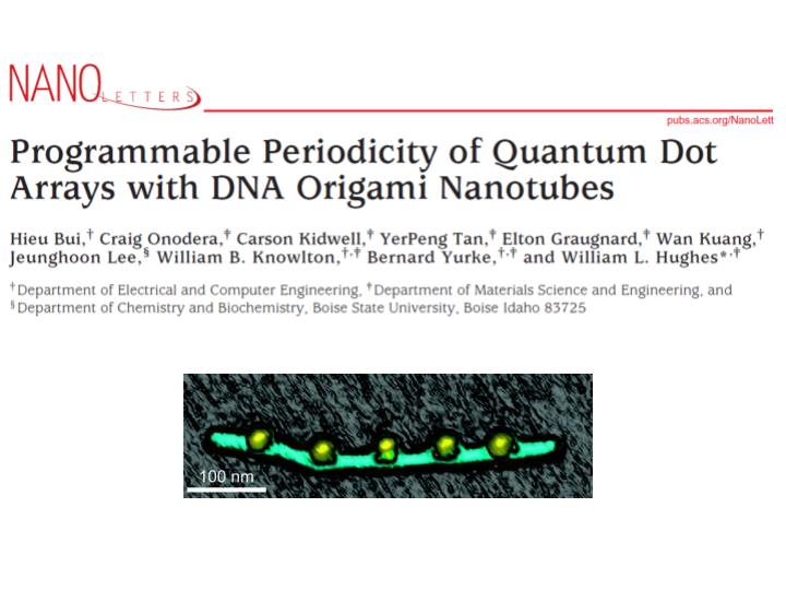
Design • One long DNA strand (black) with 170 short ‘staple’ strands (red) • (A), (B), (C) are clustered biotin • DNA forms 6-helix nanotube bundle (412 x 6 nm)
Assembly & Binding • Height = 1.7- 3.5 nm (6 nm) • Length = 436 +/- 14 nm (412 nm)
Assembly & Binding • Successful attachment of 9 streptavidin (height increase ~0.5 nm) • Periodicity of 45 nm (43 nm expected)
Assembly & Binding • QDs have similiar spacing • 5.5 nm height cross section • 49 nm periodicity
Conclusion • Powerful and convenient pathway to control nanoparticle patterning • Self-assembling scaffold for nanoscale electronic and photonic devices • Variations available for spacing, length, QD size, and QD material
Controlled Drug Deliver • Self-assembled micelles • Biocompatible and biodegradable • Amphiphilic block copolymers (PEG, PCL, PLA) • Inefficient drug release
PEG Alternative • Dextran (Dex) • Aqueous soluble, biocompatible, branching • -OH functionality for conjugation • Authors report shell-sheddable biodegradable Dex-SS-PCL micelles for drug delivery
Micelle Formation • Average micelle size increased from 60 to 200 nm with DTT addition • Aggregates from lose of solubilizing shell • Little change after 24hrs w/o DTT
Cellular Uptake 2 hr 4 hr 24 hr
Cellular Uptake Free DOX 2 hr No DOX 4 hr 24 hr
Toxicity • Free DOX and cleavable micelle show similar response • Control and non-DOX loaded micelle show similar response
Conclusion • Nontoxic Dex-SS-PCL diblock copolymers with high drug loading efficiency were developed • Micelles are stable and allow for rapid drug release in response to intracellular levels of reducing potential
Overview • Effort to mix nanoparticles (NP) with polymers to combine unique physical properties with processibility • Need efficient ways to control NP arrangement in polymer matrix • Dispersion of NP impacts electronic, transport, and mechanical properties
Conclusions • Initially NPs are randomly incorporated in swollen polymers • Polymers pack more densely with water and NPs phase segregate to polymer core-shell interface
Nano Lett., Article ASAP Publication Date (Web): January 26, 2010
Goals • Efficient, highly portable energy sources for hand-held electronics • Decreasing power requirements • Augment batteries with ‘scavenger’ systems • Salvage otherwise wasted energy
Wasted Energy… • Work by the human body • Breathing • Lung expansion/contraction generate ~1 W (charge pacemakers?) • Walking • A heel strike during walking has 67 W of power available (~1-5% energy to power cell phones)
Piezoelectrics • Crystals become electrically polarized by mechanical stress (and vice versa) • Processing - high temperature, rigid inorganic substrates • Authors present approach to incorporate crystalline piezoelectric lead zirconate titanate (PZT) onto rubber substrates for flexible energy conversion -http://www.piezomaterials.com/
Production Processed into nanothick ribbons and printed onto polydimethyl-siloxane (PDMS) stamps via dry transfer
Function • Schematic of a specimen indicating piezoelectric bending and measurement. • (b) Oscillating pressure (left axis) and induced dielectric displacement (right axis)
Summary • Highly crystalline piezoelectric ceramic ribbons have been transferred onto flexible rubber substrates • Efficient electromechanical energy converters towards wearable/implantable energy harvesters • Challenges to overcome: stretchable substrates, cycling longevity, storage/power conversion on substrates…
Light Concentration • Surface plasmons • Electromagnetic surface waves carried by density fluctuations of electrons • Patterned metals • Films, trenches, gaps, tips for control and delivery of surface plasmons
Surface Plasmons • Focusing on tip or apex allows for excitation of highly local and extremely intense optical fields • ‘Optical lightning rod’ • Authors present three-dimensional plasmonic nanofocusing with patterned gold and silver pyramids
Nanopyramids 500 nm 200 nm 500 nm 1000 nm Light incident from above is backscattered into plasmons that travel up sides and corners, converging at the apex
Fabrication • Xu, Q., Tonks, I., Fuerstman, M., Love, C., Whitesides, G. Nano Lett., 2004, 4 (12), 2509. • Henzie, J., Kwak, E., Odom, T. Nano Lett, 2005, 5 (7), 1199.
Fabrication • Xu, Q., Tonks, I., Fuerstman, M., Love, C., Whitesides, G. Nano Lett., 2004, 4 (12), 2509. • Henzie, J., Kwak, E., Odom, T. Nano Lett, 2005, 5 (7), 1199.
Conclusion • 3-D nanofocusing with well-defined plasmonic hot spots • Applications in scanning-probe microscopy, optical trapping, high-density data storage • Thin films allow for backside excitation