Download
1 / 15
150 likes | 284 Vues
VTT MICROELECTRONICS 3D RADIATION DETECTORS ORSAY SEPTEMBER 2003. STATUS AS PERFORMER OF RESEARCH AND DEVELOPMENT WORK. Basic research Applied research Development work. Universities. VTT. Industry. VTT IN BRIEF www.vtt.fi. Staff breakdown by location: Oulu 323 Outokumpu 37

E N D
VTT MICROELECTRONICS3D RADIATION DETECTORS ORSAY SEPTEMBER 2003
STATUS AS PERFORMER OF RESEARCH AND DEVELOPMENT WORK Basicresearch Appliedresearch Developmentwork Universities VTT Industry
VTT IN BRIEFwww.vtt.fi Staff breakdown by location: Oulu 323 Outokumpu 37 Jyväskylä 128 Tampere 332 Lappeenranta 12 Espoo 2 159 Others 21 Total 3 012 Units: VTT Electronics VTT Information Technology VTT Industrial Systems VTT Processes VTT Biotechnology VTT Building and Transport VTT Information Service VTT Corporate Management and Services • Staff: 3 012 • Turnover: 214 M€ • Basic govern. funding to research • on VTT’s own initiative 34 M€ • Jointly funded projects 92 M€ • Commercial activities 88 M€
VTT’S TURNOVER BY TYPE OF INCOME AND FUNDING 250 Income from commercial activities Income from jointly funded activities Basic governmental funding to jointly funded activities Basic governmental funding to research on VTT’s own initiative 200 150 40% 25% 19% 16% 40% 28% 18% 14% 39% 32% 17% 12% 39% 32% 16% 13% 40% 30% 14% 16% 41% 27% 16% 16% 100 50 0 1996 1997 1998 1999 2000 2001
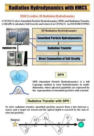
DETECTOR ACTIVITIES IN 2003 1. Products + extras 2. New detector types for imaging & xrf 3. Device and process physics for planar detectors 4. 3D-detectors
3D 3D PLANAR (strips &pixels)
DETECTOR ACTIVITIES IN 2003 3D • WHY • small voltage • high collection speed • edgeless • radiation hardness • Spatial resolution • Large area CZ-wafers APPLICATIONS: hep & imaging
DETECTOR ACTIVITIES IN 2003 3D • PROCESSING • 1. Normal processing steps applied for the planar detectors • 2. Deep hole etching • ICP-silicon etching (so called Bosch-process): established silicon process • 3. Hole filling / planarization (polished surface, wafer handling & processing) • LPCVD polysilicon or so-called epitaxial polysilicon (epi-poly) • both processes can be grown as non-doped or in-situ doped (n or p-type) • minimum resistivity: 1 mWcm-range • growth rate: LPCVD 1 mm/hour (thick layers require sequential runs), epi-poly 1 mm/min • CMP ? • 4. Dicing • important especially for so-called edgeless detectors
DETECTOR ACTIVITIES IN 2003 DETECTOR ACTIVITIES IN 2003 3D PROCESSING EXAMPLES: epi-poly Problem: void formation
DETECTOR ACTIVITIES IN 2003 3D PROCESSING: dicing • DICING BLADE: • width 20 mm • position accuracy ± 2 mm backsides doping edge doping substrate oxide metal Active strip doping Problem: thickness of damage layer
DETECTOR ACTIVITIES IN 2003 3D SIMULATIONS • 2D • Silvaco tools • mixed mode
DETECTOR ACTIVITIES IN 2003 3D 3DSIMULATIONS: ISE
DETECTOR ACTIVITIES IN 2003 3D 3D SIMULATIONS: ISE
Micro packaging • Bump bonding of detector modules for Alice, LHCb, Medipix2
Contacts • Micro packaging: Jorma Salmi, + 358 9 456 6639, jorma.salmi@vtt.fi • IC processes: Hannu Ronkainen, + 358 9 456 6660, hannu.ronkainen@vtt.fi • IC design: Markku Åberg, + 358 9 456 6619, markku.aberg@vtt.fi • MEMS: Hannu Kattelus, + 358 9 456 6319, hannu.kattelus@vtt.fi • SOI-wafers: Kimmo Henttinen, + 358 9 456 6310, kimmo.henttinen@tt.fi • Silicon detectors: Simo Eränen, + 358 9 456 6661, simo.eranen@vtt.fi