Download
1 / 13
130 likes | 255 Vues
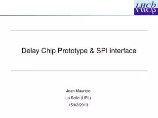
Update on DLL and slow control design. Joan Mauricio La Salle (URL) 19/12/2012. 09/02/2012. 1. Requirements. 1 ns resolution. DNL < 100 ps. 3 independent adjustable phases: ICECAL Integrator clock. ICECAL T&H clock. ADC clock. Radiation tolerant design. Policies:

E N D
Update on DLL and slow control design Joan MauricioLa Salle (URL)19/12/2012 09/02/2012 1
Requirements • 1 ns resolution. • DNL < 100 ps. • 3 independent adjustable phases: • ICECAL Integrator clock. • ICECAL T&H clock. • ADC clock. • Radiation tolerant design. Policies: ≥ 5 um between NMOS diffusion and N-Well. • Guard rings between PMOS and NMOS transistors. Slow control: • SPI. • Triple voting registers. 19/12/2012 2
VCDL Design – Basic Delay Element • Starved Inverter. • vControl is servo controlled by the Phase Comparator. • coarse is tuned externally: • Process compensation. • Duty Cycle adjust. 19/12/2012 3
VCDL Design – 1ns Delay Element ~ 330/500ps • Weak inverters ensures 180º phase between differential paths. • Output inverters isolate Delay Element from MUXs: P+ ring NMOS P+ ring N+ ring PMOS N+ ring PMOS N+ ring P+ ring NMOS 4 P+ ring
VCDL Design – 25ns Delay Line • 250 Monte Carlo simulations (Process+Mismatch): • Misamtch does not affect significantly. • DLL can be adjusted to 25 ns despite Process Variations. 5
25:1 Multiplexor and Output Buffer ~ 1100ps ~ 1500ps ~ 1500ps ~ 400ps ~ 330 / 500ps outEn • Used to choose the desired output from the VCDL. • Multiplexing is done in two steps (groups of 5). • Output Buffer reduces rise/fall time. 19/12/2012 6
25:1 Multiplexor and Output Buffer ~ 1100ps ~ 1500ps ~ 1500ps ~ 400ps ~ 330 / 500ps outEn • Used to choose the desired output from the VCDL. • Multiplexing is done in two steps (groups of 5). • Output Buffer reduces rise/fall time. 19/12/2012 7
Phase Comparator • Phase is detected by means of an XOR gate. • Flip-Flop detects phase sign. • Charge/discharge signals are generated phase and sign. 19/12/2012 8
DLL Channel Top View Phase Comp. + Charge Pump VCDL VCDL Integrator and T&H Clock generation ADC Clock generation vControl vControl LVDS2CMOS cmosClk cmosClk coarse coarse 25:1 Mux 25:1 Mux ADCClk T&HClk INTClk 19/12/2012 9
Slow Control – Triple voting Decision DFC 2,0 DFC 3,0 DFC 0,1 DFC 1,1 Decision DFC 0,0 DFC 1,0 Decision DFC 2,1 DFC 3,1 DFC 0,2 DFC 1,2 Decision DFC 2,2 DFC 3,2 • The objective is to minimize the chances of a charged particle corrupts configuration or status registers. • Interleaving factor 4 reduces the probability of 3-Voting errors. > 115 um DFC<m,n> = Flip Flop m = bit number <0,4> n = voting register <0,2> 19/12/2012 10
Slow Control – Triple voting 19/12/2012 11
Slow Control – Triple voting nRst Clk Enable In V1 V2 V3 Out 12
Slow Control – SPI ICECAL Ch = · Analog. · DLL. · Slow control. ICECAL Ch1 ICECAL Ch2 SPI Master SPI Decoder ICECAL Ch3 ICECAL Ch4 SPI Decoderinterfaceswith SPI Masterandgenerates R/W, Chip Enable, Sclk, Sdasignals for eachchannel 19/12/2012 13