Download
1 / 71
720 likes | 838 Vues
Learn about the versatile 8255A programmable peripheral interface, its modes, control register, pin diagram, operating modes, and interfacing techniques for data transfer with external devices.

E N D
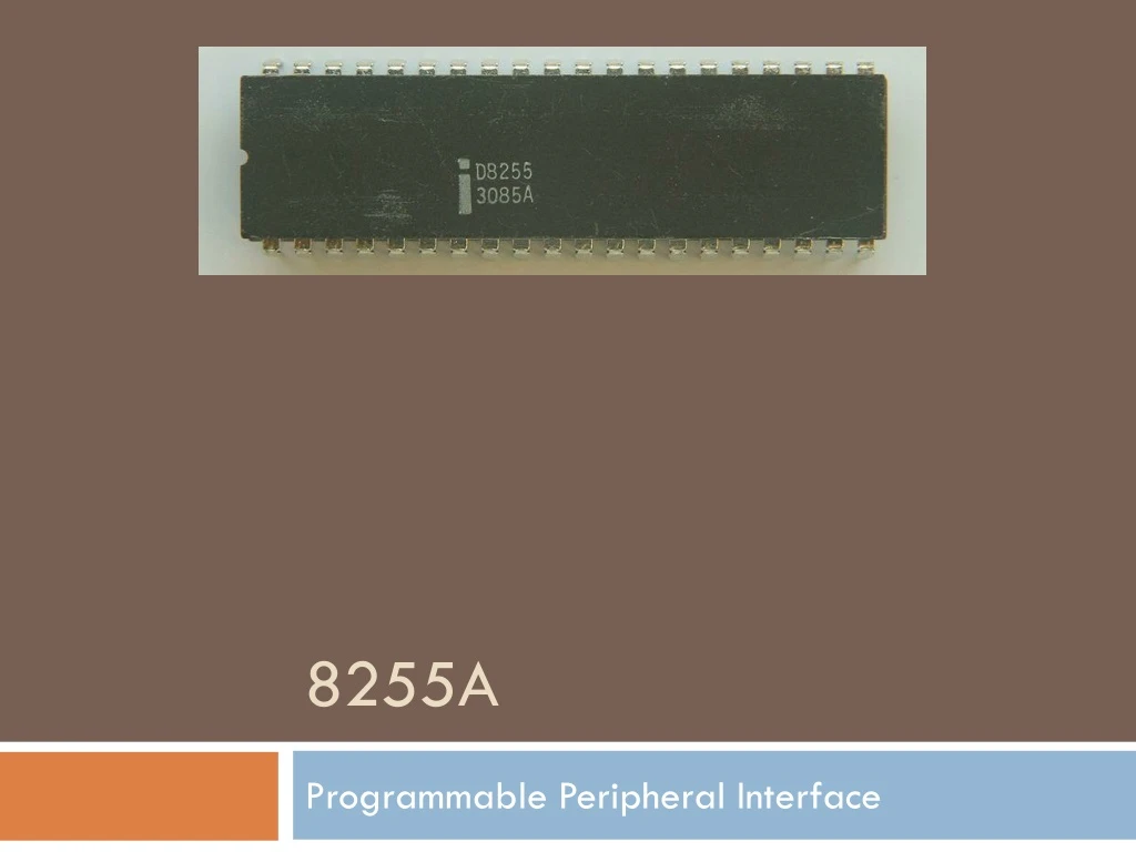
8255A Programmable Peripheral Interface
Introduction • 8255A is one of the mostly used programmable, Parallel I/O device. • It can be used to transfer the data on various conditions • When ever multiple I/O ports are required, 8255A is used for flexible interfacing between MPU and I/O peripherals
Introduction • MPU interface to external devices through both parallel and serial interfaces. • Parallel data occur in system that use: • Displays • Keyboard • Printers (old printer) • Etc. • Serial data occurs in: • Some printers • Data communications
About • 24 I/O pins • 8 bit parallel ports: A, B • C port: can be grouped as 4 bit CU(C upper) and CL(C Lower) • Two Modes: BSR(Bit Set/reset) and I/O mode • BSR mode set/reset in port C • I/O mode is further divided in 3 modes: • Mode 0: simple • Mode 1: Handshake • Mode 2 : Bidirectional
PIN Description • 8255A is having 24 I/O pins • This 24 are divided in 3, 8-bit ports(A,B,C) • Port C can be used as individual pins or it can be grouped in 2, 4-bits port (C-upper, C-lower) • The functions of this port A,B,C is been written on Control register. • RD(AL): When this signal is low, MPU reads data from selected I/O port • WR(AL): When this signal is low, MPU Writes the data into selected I/O port or Control Register • Reset : It is active high signal, it clears the bits in control register and sets all port into I/P mode.
Port address is determined to pins Ao and A1. • CS (AL) is been used to select the 8255A • If A7=1, and A6-A2=0. Ports will be having the address from 80H to 83H
Modes in 8255A • 8255A is having 2 types of operating modes • Bit SET/RESET mode :- Used to set and reset the bits in port C only • This mode will be selected when D7 bit of control register is “0”. • I/O mode: used to transfer the data. • This mode is selected when D7 bit of control register is set to “1” • Divided into 3 types • Mode 0:All ports will function as simple I/O ports • Mode 1:Hand shake Mode • Mode 2: Port A can be SET for bidirectional data transfer using handshake mechanism with port c, and Port B can be used either Mode 0 or 1.
Bit SET/RESET (BSR) • In this mode each line of port C(PC0-PC7) can SET/RESET by suitably loading the control word register.
Example As an example, if it is needed that PC5 be set, then in the control word, Since it is BSR mode, D7 = '0'. Since D4, D5, D6 are not used, assume them to be '0'. PC5 has to be selected, hence, D3 = '1', D2 = '0', D1 = '1'. PC5 has to be set, hence, D0 = '1'. Thus, as per the above values, 0B (Hex) will be loaded into the Control Word Register (CWR).
Steps for data receiving or transferring to peripheral • Mode 0 – input mode • In the input mode, the 8255 gets data from the external peripheral ports and the CPU reads the received data via its data bus. • The CPU first selects the 8255 chip by making CS low. It then selects the desired port using A0 and A1lines. • The CPU then issues an RD signal to read the data from the external peripheral device via the system data bus. • Mode 0 - Output mode • In the output mode, the CPU sends data to 8255 via system data bus and then the external peripheral ports receive this data via 8255 port. • CPU first selects the 8255 chip by making CS low. It then selects the desired port using A0 and A1lines. • CPU then issues a WR signal to write data to the selected port via the system data bus. This data is then received by the external peripheral device connected to the selected port.
8255A Programmable Peripheral Interface • Mode 0: Input / Output Mode • In this mode port A and B use 8-bit I/O data and port C uses two ports 4-bit data. • The characteristics of mode 0 are: • Output is latched. • Input does not latched. • Ports do not have the capability of handshake mode or interrupt mode.
Figure 9: • Example :
8255 PIA: Example • Solutions: • Port Address : • It is actually an I/O memory map. • When A15 is active high, Chip Select signal is activated. • Assuming all don’t care signals are at logic 0, therefore ports’ address are as follows:
8255A Programmable Peripheral Interface • Solution: • Control Word:
8255 PIA: BSR Mode • Example: • Write a BSR control word subroutine to set bit PC7 and PC3, and reset after 10ms. Use the schematic diagram as shown below.
8255A Programmable Peripheral Interface • Solution: • BSR Control Word: • Port Address: • As shown in previous example : 83H
8255A Programmable Peripheral Interface • Solution: • Subroutine: Assuming that the delay subroutine has been determined earlier.
Example • Write a program to read the DIP switches and display the reading from port B at port A and from Cl at port Cu. • Consider Port A=8000h(A1=0,A0=0) • Port B=8001H(A1=0,A0=1) • Port C= 8002H(A1=1,A0=0) • Control register=8003H(A1=1,A0=1).
Control word • D7=1, I/O function • D6,D5=00 PORT A in MODE 0 • D4=0, Port A=OUTPUT • D3=0,Port Cu=OUTPUT • D2=0, PORT B in mode 0 • D1=1, port B=input • D0=1,port Cl=Input.
MVI A,83H; load accumulator with the control word • STA 8003H; write the word in the control register to initialize the ports • LDA 8001H; Read the switches at port B • STA 8000H; Display the reading at port A • LDA 8002H; Read switches at port C • ANI 0FH; mask the upper four bits of port c. these bits are not input data • RLC • RLC • RLC • RLC • STA 8002H, Display data at port Cl • HLT
Mode 1 • This mode is same as mode 0 but only difference is port C is been used for handshaking and control. • Two ports i.e. port A and Port B can be used as 8 bit i/o port • Each port uses 3 lines of the port C as handshake signals and remaining two signals can be function as i/o port • Interrupt logic is supported.
Input control signals(handshaking signal) • Strobe input(STB(AL)): This is generated by peripheral device to indicate that it has transmitted a byte of data. In response to STB, 8255 generates IBF and INTR signals • IBF (Input Buffer Full): This indicate that input latch has received the data byte . It acknowledgement signal by 8255. • INTR(Interrupt Request): This is an o/p signal that is used as interrupt to MPU. • INTE( Interrupt Enable): This internal flip-flop , which is been used to enable or disable the generation of INTR signal.
Application of MODE 1( Keyboard as input and output as printer) • Find port addresses by analyzing the decode logic • Determine the control word to setup port A as input and port B as output in mode1 • Determine the BSR word to enable INTEa(port A) • Determine the masking byte to verify the OBFb(AL) line in the status check I/O(PORT) • Write initialization instructions and printer subroutine to output characters that are stored in memory
Instruction to display on LED DISPLAY • MVI A, DATA; load accumulator with data • OUT FFH; output accumulator contents to port FFH • HLT ; end the program
Mode 1: Input or Output with Handshake • In this mode, handshake signals are exchanged between the MPU and peripherals prior to data transfer.
Mode 1: Input or Output with Handshake • The features of the mode include the following: • Two ports (A and B) function as 8-bit I/O ports. • They (A and B) can be configured as either as input or output ports. • Each port uses three lines from Port C as handshake signals. • The remaining two lines of Port C can be used for simple I/O operations. • Input and Output data are latched. • Interrupt logic is supported.
Signal Description • STB- Strobe input: (active low) : generated by peripheral to indicate it has transmitted the data. • IBF( Input buffer full) : Acknowledged by 8255 to indicate the input buffer has received the data. • INTR( Interrupt Request) : This is output signal that is used to INTR the uP. • This is high when STB , IBF and INTE(internal signal) is high. • INTE (Interrupt Enable): internal flip flop