Download
1 / 66
660 likes | 811 Vues
Basic Fundamentals of Solar Cell Semiconductor Physics for High School Level Physics. Review Topics. Wavelength and Frequency. Period (sec). amplitude. time. Frequency ( n ) = 1/Period [cycles/sec or Hertz] Wavelength ( l ) = length of one Period [meters]

E N D
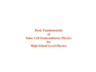
Basic Fundamentals of Solar Cell Semiconductor Physics for High School Level Physics
Wavelength and Frequency Period (sec) amplitude time Frequency (n) = 1/Period [cycles/sec or Hertz] Wavelength (l) = length of one Period [meters] For an electromagnetic wave c = nl,where c is the speed of light (2.998 x 10⁸ m/sec)
Spectrum Intensity Frequency (n) Range of frequency (or wavelength, c/n) responses or source emissions. The human eye has a response spectrum ranging from a wavelength of 0.4 microns (0.4 x 10⁻⁶ meters) (purple) to 0.8 microns (red)
Energy and Power Electromagnetic waves (light, x-rays, heat) transport energy. E = hn or hc/l [Joules or eV (electron-volts)] 1 eV = 1.6 x 10⁻¹⁹ Joules h = Plank’s constant (6.625 x 10⁻³⁴ Joule-sec or 4.135 x 10⁻¹⁵ eV-sec) n = frequency c = speed of light l = wavelength Power is the amount of energy delivered per unit time. P = E/t [Joules/sec or Watts]
Photons A light particle having energy. Sunlight is a spectrum of photons. X-rays and heat are photons also. Photon Energy E = hn or hc/l [Joules or eV (electron-volts)] (higher frequency = higher energy) (lower energy)
Irradiance Amount of power over a given area, Watts/m2 4 red photons every second Area = 2.00 m2 Energy of 1 red photon = hc/l = (6.63 x 10⁻³⁴ J-s)(2.99 x 10⁸ m/s)/(0.80 x 10-6 meters) = 2.48 x 10⁻¹⁹ J = 1.55 eV Irradiance = Power/Area = (4 photons/sec)(Energy of 1 photon)/2.00 m2 = 4.96 x 10⁻¹⁹ W/m2 Typical sunlight irradiance is 0.093 W/cm2 = 930 W/m2 at l = .55 mm
Transmission, Reflection, and Absorption incident light reflectance (R) air transmittance (T) + absorptance (A) material • Incident light = T + R + A = 100% • Non-transparent materials have either very high • reflection or very high absorption. • Absorption decreases transmission intensity with • increasing depth into material.
Polarization Polarizer Unpolarized light (e.g. sunlight) Linearly polarized light Only one plane of vibration passes
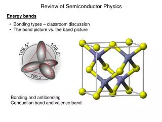
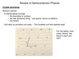
Semiconductor Crystal Lattice atom covalent bond Simple Cubic Structure Silicon has a more complex lattice structure but a lattice structure exists nevertheless.
Crystalline Silicon Bonds valance electrons Si atom (Group IV) = covalent bond (electron sharing)
+ Breaking of Covalent Bond Creating Electron-Hole Pair free electron moving through lattice e- created hole (missing electron) covalent bond Si atom Photon (light, heat) Photon hits valance electron with enough energy to create free electron
+ + Movement of a Hole in a Semiconductor Thermal energy causes valance electron to jump to existing hole leaving a hole behind
e- + Valance and Conduction Energy Bands free electron moving in lattice structure Conduction Energy Band Ec Band Gap Energy, Eg = Ec - Ev Valance Energy Band Ev Hole within valance band covalent bonds
Valance and Conduction Energy Bands Thermal Equalibrium e- e- + + free electron combines with hole free electron within lattice structure Conduction Energy Band Ec Eg Heat enery given up Heat energy absorbed Valance Energy Band Ev Hole created within valance band covalent bonds Energy absorbed = Energy given up
e- + Intrinsic (pure) Silicon Electron-Hole Pairs Thermal Equalibrium ni = 1.5 x 1010 cm-3 at 300° K Conduction Band Ec hole density = electron density number of holes per cubic centimeter = number of free electrons per cubic centimeter pi = ni = 1.5 x 1010 cm-3 Eg = 1.12 eV pi = 1.5 x 1010 cm-3 at 300° K Valance Band Ev covalent bonds • Number of electron-hole pairs increase with increasing temperature • The thermal voltage, Vt is equal to kT/e (k = 8.62 x 10⁻⁵ eV/K, T = [Kelvin])
Doping or Substitutional Impurities Group V Atom (Donor or N-type Doping) Phospherous (Group V) P atom e- covalent bond Si atom (Group IV) The donor electron is not part of a covalent bond so less energy is required to create a free electron
e- e- + Energy Band Diagram of Phospherous Doping intrinsic free electron donor free electron Conduction Band Ec Donor Electron Energy n > p (more electrons in conduction band) A small amount of thermal energy (300° K) elevates the donor electron to the conduction band Eg Ev Valance Band intrinsic hole covalent bonds N-type Semiconductor
- + Doping or Substitutional Impurities Group III Atom (Acceptor or P-type Doping) Boron (Group III) B atom covalent bond created hole covalent bond Si atom Boron atom attacts a momentarily free valance electron creating a hole in the Valance Band
e- e- + + Energy Band Diagram of Boron Doping intrinsic free electron Conduction Band Ec p > n (more holes in valance band) A small amount of thermal energy (300° K) elevates the acceptor electron to the Acceptor band Eg acceptor electron Acceptor Electron Energy Ev Valance Band created hole intrinsic hole covalent bonds P-type Semicondutor
Charge Transport Mechanisms within a Semiconductor • Drift Current Density • Diffusion Current Density
e- e- e- e- e- e- e- e- e- + + + + + + + + + Applied Electric Field Current The number of holes or electrons passing through a cross sectional area, A, in one second x y I = q/t [I] = [coulombs/sec] = [amps] • holes move in Current direction • electrons move in opposite direction and Direction of Current
e- e- e- e- e- e- e- e- e- + + + + + + + + + Applied Electric Field Current Density The number of holes or electrons passing through a cross sectional area, A, in one second divided by A x A (area) = xy cm2 y I (amps) = coulombs/sec J (current density) = I/A [J] =[amps/cm2] and Direction of Current
e- + Applied Electric Field Drift Velocity The average velocity of a hole (vp) or electon (ve) moving through a conducting material dp Scattering Sites vp = dp/t1 dn ve = dn/t1 • Scattering Sites are caused by impurities and thermal lattice vibrations • Electrons typically move faster than holes (ve>vp)
Drift Velocity and Applied Electric Field • Newton’s Second Law of Motion • F = ma • Analogy with Electic Fields • m q (mass charge) • a E (accelerating field applied electric field) • F = qE • Without scattering sites, the charged particle • would undergo a constant acceleration. • Scattering sites create an average drift velocity. • Similar to the terminal velocity of a falling object • caused by air friction.
Drift Velocity and Applied Electric Field (cont’d) • F = qE • The force, F, on a charged partical is proportional to the • electric field, E • Scattering sites create an average drift velocity, vp or ve • The average drift velocity is proportional to the applied • electric field • vp = μpE • ve = -μnE (negative sign due to electrons moving in opposite • direction of applied electric field) • where μp and μn are constants of proportionality
Hole and Electron Mobility μp is the hole mobility in the conducting material μn is the electron mobility in the conducting material The units of mobility, μ, are v = μE [cm/sec] = [μ] [volts/cm] [μ] = [cm2/volt-sec] Typical mobility values in Silicon at 300° K: μp = 480 cm2/volt-sec μn = 1350 cm2/volt-sec
Mobility and Current Density Relation • Current • I = q/t • q = number of charged particles passing through a cross sectional • area • t = time • Current Density • J = I/A = (q/t)/A • A = cross sectional area • p = number of holes per cubic centimeter (hole density [1/cm3]) • n = number of electrons per cubic centimeter (electron density [1/cm3]) • Each hole has an average velocity of vp • Each electron has an average velocity of ve
vp + + + + + + + + + + Mobility and Current Density for Holes E x x vp y y z z Each hole has traveled a distance z in a time t = z/vp The number of holes in the volume is pV (hole density x volume) The charge of each hole is e (1.6 x 10⁻¹⁹ coulombs) I = q/t = e(pV)/(z/vp) = ep(xyz)/(z/vp) = ep(xy)vp = epA μpE Jp|drf = Ip/A = epμpE
ve ve e- e- e- e- e- e- e- e- e- e- E Mobility and Current Density for Electrons x x y y z z Replacing p with n and vp with ve gives: The charge of each electron is -e (-1.6 x 10⁻¹⁹ coulombs) I = q/t = -epV/(z/ve) = -ep(xyz)/(z/ve) = -ep(xy)ve = -epA(-μnE) I = epA(μnE) Jn |drf = In/A = enμnE
Drift Current Density Expressions Jp|drf = Ip/A = enμpE Jn|drf = In/A = enμnE Jp|drf and Jn|drf are in same direction Total Drift Current = Jp|drf + Jn|drf
Diffusion Process gas filled chamber empty chamber gas sealed membrane After seal is broken Gas molecules move from high concentration region to low concentration region after membrane is broken If gas molecules are replaced by charge then a current exists during charge transport creating a Diffusion Current
Electron Diffusion Current electron flow slope = Dn/Dx Electron concentration, n Electron diffusion current density x distance • electron flow is from high to low concentration (-x direction) • electron diffusion current density is in positive x direction • Jn|dif = eDnDn/Dx where Dn is the electron diffusion constant
Hole Diffusion Current hole flow slope = Dp/Dx Hole concentration, p Hole diffusion current density x distance • hole flow is from high to low concentration (-x direction) • hole diffusion current density is in negative x direction • Jp|dif = -eDnDp/Dx where Dp is the hole diffusion constant
Diffusion Currents • Jn|dif = eDnDn/Dx • Jp|dif = -eDnDp/Dx • Electron and hole diffusion currents are in opposite directions • for the same direction of increasing concentration Total Diffusion Current =Jn|dif - Jp|dif
Formation and Basic Physics of PN Junctions
PN Junction Formation Masking Barrier Boron Atom Doping Phophorous Atom Doping Intrinsic Silicon Wafer • Doping Atoms are accelerated towards Silicon Wafer • Doping Atoms are implanted into Silicon Wafer • Wafer is heated to provide necessary energy for Doping Atoms to become • part of Silicon lattice structure
PN Junction in Thermal Equilibrium (No Applied Electric Field) Space Charge Region metallurgical junction metallurgical junction - - - - + + + + P-type N-Type p n Initial Condition E field Equilibrium Condition • Free electrons from n-region diffuse to p-region leaving donor atoms behind. • Holes from p-region diffuse to n-region leaving acceptor atoms behind. • Internal Electric Field is created within Space Charge Region.
PN Junction in Thermal Equilibrium (No Applied Electric Field) Diffusion Forces = E Field Forces Space Charge Region metallurgical junction - - - - + + + + p n E field Diffusion force on holes Diffusion force on electrons E field force on holes E field force on electrons
Definition of Electric Potential Difference (Volts) d Positive test charge, +q0 E field x=a x=b Work (energy) per test charge required to move a positive test charge, +q, a distance x=d against an electric field, DV = (Vb - Va) = Wab/q0 =E(b - a) = Ed [volts or Joules/coulomb]
PN Junction in Thermal Equilibrium Electric Field metallurgical junction Space Charge Region p n - - - - - - - - - + + + + + + + + + - - - - - - - - - + + + + + + + + + - - - - - - - - - + + + + + + + + + E = 0 E = 0 - - - - - - - - - + + + + + + + + + - - - - - - - - - + + + + + + + + + Internal E field direction E - xp x = 0 + xn
PN Junction in Thermal Equilibrium Built-in Potential, Vbi metallurgical junction Space Charge Region p n - - - - - - - - - + + + + + + + + + - - - - - - - - - + + + + + + + + + - - - - - - - - - + + + + + + + + + E = 0 E = 0 - - - - - - - - - + + + + + + + + + - - - - - - - - - + + + + + + + + + Internal E field direction V Positive test charge, +q0 DV = Vbi - xp x = 0 + xn
Conduction and Valance Band Diagram for PN Junction in Thermal Equilibrium Built-in Potential, Vbi Ec eVbi Ec Ev Ev p region space charge region n region - xp x = 0 + xn
------ ----- ---- Conduction Band Diagram for PN Junction in Thermal Equilibrium Electron Energy Ec eVbi Ec - xp x = 0 + xn p region space charge region n region Work or Energy is required to move electrons from n region to p region (going uphill)
Applying a Voltage Across a PN Junction Non-Equilibrium Condition (external voltage applied) Reverse Bias Shown Increased Space Charge Region metallurgical junction - - + + + + + ++ ++ + - - - - n p - - E field Forward Bias - - E applied + - Reverse Bias Vapplied + - • Eapplied is created by bias voltage source Vapplied. • Efield exists in p-region and n-region. • Space Charge Region width changes. • Vtotal = Vbi + Vapplied
Reverse Bias PN Junction Non-Equilibrium Condition (external voltage applied) Increased Space Charge Region metallurgical junction - - + + + + + ++ ++ + - - - - n p - - E field - - Ireverse E R + - VR • ER is created by reverse bias voltage source VR. • ER is in same direction as internal E field. • Space Charge Region width increases. • Vtotal = Vbi + VR • Ireverse is created from diffusion currents in the space charge region
Conduction and Valance Band Diagram for PN Junction Reverse Bias Voltage Applied Vtotal = Vbi + VR Ec eVbi + eVR Ec space charge region Ev p region n region Ev - xp x = 0 + xn