Download
1 / 18
190 likes | 387 Vues
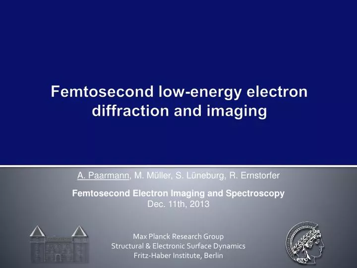
Femtosecond low-energy electron diffraction and imaging. A. Paarmann , M. Müller, S. Lüneburg, R. Ernstorfer Femtosecond Electron Imaging and Spectroscopy Dec. 11th, 2013. Acknowledgements. FHI Berlin Max Planck Research Group “Structural and Electronic Surface Dynamics”.

E N D
Femtosecond low-energy electrondiffraction and imaging A. Paarmann, M. Müller, S. Lüneburg, R. Ernstorfer Femtosecond Electron Imaging and Spectroscopy Dec. 11th, 2013
Acknowledgements FHI Berlin Max Planck Research Group “Structural and ElectronicSurface Dynamics” • Nanometer Structure Consortium, Lund University Magnus Borgström Martin Hjort Anders Mikkelsen Lars Samuelson Melanie Müller Sebastian Lüneburg Ralph Ernstorfer
Ultrafast Electron Diffraction & Microscopy Pump-probe: Ultrafast temporal resolution Diffraction / Microscopy: Structural (atomic) resolution + time scale: 100 fs length scale : Å … nm 10 MeV Relativisticelectrondiffraction Transmission electronmicroscopy 1 MeV Gas phase electrondiffraction Transmission electrondiffraction 100 keV Scanning electronmicroscopy Electronenergy Reflection high-energy electrondiffraction Charge per pulse 10 keV 1 keV Low-energy electrondiffraction / microscopy + High surfacesensitivity +/- Very sensitive toelectricfields + Little sample damage 100 eV
Major Challenge at Low Energies:Electron Pulse Duration Delivering < 100-fs electron pulses at sub-kV energies is a big challenge ! Space charge Vacuumdispersion • Time-resolved experiments: • Short propagation time → Compact design • Single / few electron pulses at high rep-rate Nanotips as electron gun ! First time-resolved LEED: Karrer, Osterwalder et al.,Rev. Sci. Instrum., 72 , 4404 (2001) 4
Electron Pulse Duration: Simulations 0 0.9 0 tip dispersion Utip = -200 V d = 100 mm E0 = 0.5 eV path length difference sample 5 Paarmann et al., J. Appl. Phys. 112, 113109 (2012)
Beam CollimationforDiffraction:‚Lens Behind theTip‘ Macrolens Paarmann et al., J. Appl. Phys. 112, 113109 (2012) Lüneburg et al., Appl. Phys. Lett.103 , 213506 (2013) Microlens • Collimation (Focussing) due to plate-capacitor-like field lines • Typically < 5 mm spotsize on the sample • suppression of DC fieldenhancement + current • Disadvantage: dispersive pulse broadeningenhanced Utip = -100 V U ≤ -100 V U > -100 V
Experimental Concepts Time-Resolved Low-Energy ElectronDiffraction(trLEED) Time-Resolved Point Projection Microscopy (trPPM) • Atomic structural dynamics with high surface sensitivity • Ultrafast dynamics in 2D and quasi-2D systems • Ultrafast imaging of nano-scalesystems • Spatially resolved probing of • transient electric fields 7
Experimental Setup • Ti:Sa oscillator • 80 MHz, 2 nJ, 5 fs • Cavity dumped Ti:Sa • 1 MHz, 30 nJ, 16 fs • Regenerative Ti:Sa amplifier • 200 kHz, fewmJ, 50 fs 0.18 e-/pulse 100 nm
Point Projection Imaging with fs-Electron Pulses 60 nm gold nanowires on quantifoil (2 μm holes) DC fieldemission Laser-triggeredemission
Transmission LEED of single-layergraphene Unpublished data …
Space Charge Dynamics • Generate space charge from a metal surface/edge and detect deflection of the probe electron beam • Pt pinhole • Cu TEM grid edge
Space Charge Dynamics Unpublished data …
Space charge dynamics Unpublished data …
Transient Electric Fields at Photoexcited Semiconductor Nanowires • time-resolved Point projectionmicroscopy • SemiconductingInPnanowires • Diameter: 30 nm, length: 1.5 μm • Placed on quantifoilsubstrate Hjort et al., ACS Nano 6, 9679 (2012)
NanowireLocal Field Dynamics Unpublished data …
NanowireLocal Field Dynamics Unpublished data …
Outlook: „Divergent Beam LEED“ Unpublished data …
Summary • Extremely compact, versatile machine for time-resolved low-energy electron diffraction and microscopy • Large scattering cross section of low energy electrons • Best suited for low-dimensional systems • High sensitivity to local electric fields • First observation of real-space local field dynamics at semiconductor nanowires • Resolution in microscopy mode: < 200 fs, ~ 30 nm • Resolution in diffraction mode: < 2 ps, < 0.02 Å-1 Thanksforyourattention!