Download
1 / 189
1.96k likes | 2.19k Vues
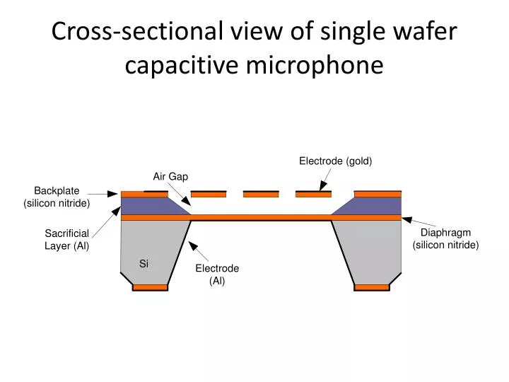
Cross-sectional view of single wafer capacitive microphone.

E N D
One of the earlier microphones was designed by Scheeper et al. in 1991. The design is based on using a single silicon wafer with a 1 µm-thick layer of LPCVD nitride grown on each side. The nitride was then patterned and etched in KOH. On the top side of the wafer, aluminum was evaporated as a sacrificial layer which was between 1 and 3 microns thick. Another micron-thick layer of nitride was grown on top of the aluminum layer using PECVD. Then an adhesion layer of 30 nm titanium was evaporated on the surface, followed by the addition of the gold electrode. After patterning, the acoustic holes were etched in the Ti/Au layers and in the PECVD nitride. Using the acoustic holes, the aluminum sacrificial layer was etched. Finally, the last step of the fabrication was to evaporate 100 nm of aluminum on the bottom side of the wafer.
(a) Growth of 1 pm LPCVD silicon nitride. patterning and anisotropic etching of V grooves and diaphragm in 33wt.% KOH solution (73'C). • (b) Evaporation of 3pm aluminium, growth of 1 um PECVD silicon nitride, evaporation and patterning of a 30nm titanium adhesion layer and a 30nm gold electrode, etching of accesslacoustic holes in TilAu and PECVD silicon nitride. • (c) Etching of aluminium sacrificial layer, drying and evaporation of lOOnmaluminiumon siliconlsiliconnitride on the reverse side (counter electrode)
This microphone consists of a rigid 20 µm thick monocrystalline silicon back plate with acoustic holes, a 0.3 µm thick metallized low stress LPCVD silicon nitride membrane, and an air gap of 1.3 µm produced by a sacrificial layer of porous silicon and SiO2.
This microphone was made from a double-sided polished p-doped silicon wafer. The first fabrication step was to p+ doped both sides of the wafer. A thin nitride layer was deposited by LPCVD for use as a mask for the porous silicon formation. The porous silicon was created in a portion of the heavily p-doped silicon by etching in 25% HF and 50% ethanol in water. An electrical current was then sent through the porous silicon formation. The next step was to remove the masking layer and then sputter a 0.8 micron oxide layer onto the top side of the wafer. The oxide and the porous silicon would later be used as the sacrificial layer to create the air gap. Then a 300 nm layer of nitride was deposited with LPCVD on both sides. The nitride was used as a masking layer to create contact holes on the front side and windows on the back side of the wafer. After patterning the nitride by a mask, the holes and backside were etched in KOH. Aluminum was deposited on the front and back of the wafer to act as an RIE etch mask and a conductive layer (Linder et al. 1996). Acoustic holes were etched into the backplate to reach the porous silicon by RIE in SF6 plasma. The porous silicon was etched with KOH, and then the oxide layer was etched with HF. This last etching step releases the nitride diaphragm.
Cross-sectional view of a condenser microphone with polyimide
In this microphone, the diaphragm and back plate are made of a polymer (polyimide). In this microphone, the silicon substrates used were 3”, <100>, p-type, 5 Ω cm wafers. The thickness of the substrates was 400 μm. First, a 1.5 μm thick layer of SiO2 was grown by wet oxidation at 1150 oC. The SiO2 was subsequently etched in BHF to define the active sensor area on the backside of the substrate. During the etching, the front was protected with photoresist. The substrate was then etched in a KOH solusion (33 wt.%, 73 oC) until the thickness in the sensor area was reduced to approximately 50 μm. After rinsing, a thin diaphragm electrode was evaporated and patterned on the front, using a standard lift-off process with photoresist. The electrode was a Cr/Au/Cr multilayer, with a thickness of 4/20/4 nm.
The first layer of polyimide, which is later to be the diaphragm, was then spun on the front. The polyimide was then cured for 1 h at 300 oC in an N2 atmosphere, and the thickness of the polyimide diaphragm was measured to be 0.8-0.9 μm. An Al sacrificial layer was then deposited and patterned, using electron-beem evaporation and a standard Al etch solution. The thickness of the sacrificial layer was 1.5 μm. Subsequently, the backplate electrode was deposited and patterned using resistive evaporation and lift-off. The thickness of the CR/Au/Cr multilayer electrode was 10/200/10 nm. After rinsing the substrate, the polyimide backplate layer (~18 μm) was spun on to the front. The sacrificial Al layer was then etched for 3 h using the standard Al etch solution. The final step was to release the polyimide diaphragm by etching the remaining silicon under the diaphragm
Cross section of the polysilicon diaphragm condenser microphone
A condenser microphone using a polysilicon diaphragm has been presented by Hsu et al. in 1998. The device consists of an n-type silicon substrate, a thin low-stress phosphorus doped polysilicon diaphragm, a P+ perforated back plate, and the metal contacts. To fabrication of this microphone, on (100) n-type silicon wafers, a 1 μm thick wet oxide is first grown at 1100 oC for 3 h. This oxide layer is patterned and etched in the buffered HF (5:1 BHF) for 12 minutes serving as a mask for the deep boron diffusion. A deep P+ boron diffusion is next introduced into the silicon from a solid source at 1175 oC for 15 h. followed by 20 minute wet oxidation at 1000 oC. The thick boron diffusion forms the stationary back electrode and the measured thickness is about 13 μm. The oxide was then stripped in a 1:1 HF: H2O solution for 4 minutes.
A 2 μm thick layer of LPCVD low-temperature oxide (LTO) is deposited at 420 oC for 4 h and patterned in 5:1 BHF for 23 minutes. This oxide provides isolation for the two electrodes. A 0.3 μm thick layer of low stress LPCVD SiN is deposited at 875 oC. This layer is patterned and etched in hot phosphoric acid for 3 h using a 0.5 μm layer of LTO as a mask. This nitride layer protects the passivation oxide from a subsequent the sacrificial etch. A 4 μm thick LTO sacrificial layer is next deposited defining the air gap electrode spacing. This oxide is patterned and etched 5:1 BHF for about 20 minutes.
Next, a 2 μm thick layer of LPCVD low-stress polysilicon is deposited at 588 oC. This material showed an unannealed tensile residual stress of about 100 MPa. The deposition is followed by a phosphorus ion implantation of 7x1015 cm-2 at 50 KeV. The remaining 1 μm thick layer of polysilicon is next deposited. The polysilicon is next annealed at 1050 oC for 1 h to redistribute the diaphragm dopants and remove as much residual stress as possible. The poly layer is next patterned and etched first using RIE with 20:5 SF6:O2sccm, at 40 mT, and 60 W for 15 minutes, followed by a wet etch in 950:500:50 NHO3:H2O: NH4F for 25 minutes.
A 0.6 μm thick LTO mask is deposited and patterned in BHF for 7 minutes to define the contact area of the back plate. The nitride over the contact area is then etched in hot phosphoric acid for 3 h. A second 0.5 um thick LTO layer is deposited followed by a 0.2 um Al evaporation. The LTO protects the front side of the wafer during the backside etch and the metal is used to pattern the back to front alignment key. The backside oxide is patterned and etched in 5:1 BHF for about 8 minutes. The wafer is then anisotropically etched in EDP for 8 h at 110 oC. After striping the protective LTO in 5:1 BHF for 20 min., the wafers are dried. Cr and Au are next evaporated forming the contact pads with thickness of 50 and 400 nm. The metal is next patterned and wet Au and Cr etchants for 4 and 1 min, respectively. Finally, the device is released in concentrated HF for 1 h. in this operation, the HF removes the sacrificial LTO from the backside while the wafer front is protected by the SiN layer
The component consists of a low-stress polysilocon bending diaphragm and a high-stress polysilcon perforated back plate that are separated by an air gap. The lower membrane bends due to a pressure difference, while the perforated membrane remains steady and the capacitance between the membranes changes.
The components were fabricated by combining the bulk and surface-micromachining techniques. First, double-sided polished 4-in. p-type 100 silicon wafers were thermally oxidised. The oxide serves as an electrical insulator for the electrodes and as a masking and stopper layer in TMAH etching. A polysilicon layer for the bending membrane was then deposited using the standard LPCVD and patterned with RIE plasma etching. A sacrificial TEOS oxide layer was deposited and small holes for anti-sticking spikes were etched. The idea behind the anti-sticking spikes is to reduce the contact area between the membranes. Next, a second polysilicon layer for the perforated membrane was deposited and patterned. An LPCVD silicon nitride layer was deposited for top insulation, and contact holes for the electrodes and the substrate were etched through the nitride and oxide layers. Before the etching in TMAH, the silicon substrate, a protective LTO oxide layer was deposited on the front side of the wafers, and the thermal oxide at the backside was patterned using a double-sided lithography. After the TMAH etching, the sacrificial oxide layers were etched in a PSG etch. PSG etch was used instead of HF due to its better selectivity with respect to aluminium. The wafers were rinsed in water and tertiary butanol and dried using freezing and sublimation. Finally, the wafers were diced into chips by cleaving along the v-shaped grooves formed in the TMAH etching step.
The device used a polysilicon Germanium diaphragm, an air gap and a gold-coated nitride back plate. The process starts with a <100> oriented n-type silicon wafer. A 1.0 micron thick silicon nitride, Si3N4, layer is deposited by LPCVD process. Over the nitride layer, a 30 nm thick layer of titanium is sputtered, which is followed by the evaporation-deposition of a 30 nm thick layer of gold. Next, a four micron thick layer of thermal oxide is deposited and then patterned. This is next followed by the deposition of a 300 nm thick layer of low-stress PECVD SiN layer. This nitride layer will act as an isolator between the poly SiGe diaphragm and the backplate electrode (Chowdhury et al. 2002).
The PECVD nitride layer is then patterned and etched in hot phosphoric acid using a 0.5 μm thick layer of low temperature oxide. In the next step a 40 nanometer thick layer of polysilicon is deposited by LPCVD process. This polysilicon layer will act as the nucleation layer for the subsequent deposition of polysilicon germanium (poly SiGe). The poly SiGe (30% Ge) is deposited by LPCVD process using SiH4 and GeH4 gases. The poly SiGe layer is then ion-implanted with phosphorous and annealed at 925 oC to reduce the residual stress. The poly SiGe layer is then patterned and etched using reactive ion etching with SF6/CH4 plasma. After that a thin layer of low-temperature oxide is deposited and patterned in Buffered Hydrofluoric acid (BHF) to define the contact hole for the backplate (gold electrode).
The nitride over the contact area is then etched by hot phosphoric acid. Next, the backside of the wafer is patterned using a 0.5 μm thick layer of low temperature oxide (LTO). The silicon wafer is then etched using SF6/O2 plasma. Next, the silicon nitride backplate is patterned using LTO and the silicon nitride layer and titanium layer are plasma etched using CF4/O2. The gold layer is then RIE etched using Cl2. The protective LTO is then stripped. Chromium and Gold are next evaporated to form contact pads with a thickness of 50 and 400 nm, respectively. The contact pads are then patterned and wet etched. Finally, the sacrificial thermal oxide layer is etched by BOE to release the diaphragm and then the wafer is freeze-dried using cyclohexane at atmospheric pressure under a continuous flow of nitrogen
Fabrication Process of the Capacitive Structure • The process uses five masks and starts with a double side polished p-type (100) silicon wafer as a substrate. • First a 4-inch p-type (100) silicon wafer is cut into several pieces to be used as substrate. • Each of the samples should be cleaned using standard cleaning procedure to remove organic contaminants such as dust particles, grease or silica gel and then remove any oxide layer from the wafer surface prior to processing. • The first step in the cleaning process is to clean the wafer using ultrasonic in the acetone solution for 5 minutes. • The second step is to put the samples into the methanol solution using ultrasonic for 5 minutes. • Final step is to dip the samples in a 10:1 DI water-HF solution (10% HF) until hydrophobic (i.e. no water can stick to wafer). This will remove native oxide film.
Fabrication process for DRIE of silicon wafer • A 300-μm-thick (100)-oriented silicon wafer isused for the substrate. • In step (1), a 300 nm-thick Al, which is a masking material for DRIE, is evaporated on surface of the silicon wafer. • In step (2), approximately 1.5 μm of thin positive photoresist (AZ-1500) was spin-coated on the Al surface. • In step (3), it was exposed for 10 sec using a contact mask aligner with a UV light source. • In step (4), it was developed for 60 seconds in AZ 300 MIF. • In step (5), Al was wet etched for 17 seconds in 10% hydrofluoric acid (HF) solution. • In step (6), the Photoresist layer was removed in acetone. • In step (7), a 260 μm deep cavity was fabricated in the silicon wafer by the DRIE system. • In step (8), the Al thin film is removed by 10%HF solution.
A 0.5 µm thick wet oxide is grown on silicon wafer. • This oxide layer is patterned and etched in the buffered HF (6:1 BHF) serving as a mask for the phosphorus diffusion. • A n+ phosophorous diffusion is next introduced into the silicon wafer as a back plate electrode. The doped area acts as a back plate electrode. • A constant source diffusion process was used to obtain the n+-silicon layer with a depth of 0.4 µm and surface concentration as high as 1020 atoms/cm3. • It was performed at 1000 oC for 30 minutes in N2 environment. • After diffusion step, the wafer was dipped in a buffered oxide etch (BOE) to remove any silicon dioxide grown during the diffusion.
Next, a Silicon-On-Glass (SOG) of 1.5 μm thick was spun with spin coater in order to form a sacrificial and insulating layer between diaphragm and back plate electrode. • The layer was gradually hot plate baked from 20 oC to 180 oC for 5 minutes and after 4 minutes gradually cooled down.
The isolating layer is then patterned and etched in PAD etch solution for 3.5 minutes to define the contact area on the back plate.
After that, a 3 m thick layer of Al is evaporated on SOG as a material of diaphragm. • The Al layer is then patterned using photoresist mask (AZ1500) to define the geometry of the diaphragm (0.5 mm x 0.5 mm), contact pad (250 µm x 250 µm), anchors and to form the circular acoustic holes (radius = 10 µm).
The holes in the diaphragm are etched by Al etchant for 33 minutes. • Finally, the sacrificial oxide layer is etched through the acoustic holes in PAD etch for 70 minutes to release the diaphragm, • The fabrication process is completed by the release of the diaphragm by immersing it in deionized water (DI) and then acetone.
Then the whole structure is dried on hot plate at 60 oC for 90 seconds to protect the diaphragm from sticking to the back plate.
Gallium arsenide (GaAs) • Gallium arsenide (GaAs) is a compound of the elements gallium and arsenic. • It is a III/Vsemiconductor, and is used in the manufacture of devices such: • infraredlight-emitting diodes, • laser diodes, • solar cells • HEMT transistors
Preparation • Gallium arsenide can be prepared by direct reaction from the elements: • Crystal growth using a horizontal zone furnace in the Bridgman-Stockbarger technique, in which gallium and arsenic vapors react and free molecules deposit on a seed crystal at the cooler end of the furnace. • Liquid encapsulated Czochralski (LEC) growth is used for producing high purity single crystals that exhibit semi-insulating characteristics.
Alternative methods for producing films of GaAs • VPE reaction of gaseous gallium metal and arsenic trichloride: 2 Ga + 2 AsCl3 → 2 GaAs + 3 Cl2 • MOCVD reaction of trimethylgallium and arsine: Ga(CH3)3 + AsH3 → GaAs + 3 CH4 • Molecular beam epitaxy (MBE) of gallium and arsenic: 4 Ga + As4 → 4 GaAs or 2 Ga + As2 → 2 GaAs
Etching • Wet etching of GaAs industrially uses an oxidizing agent such as hydrogen peroxide or bromine water.
Comparison with siliconGaAs advantages • It has a highersaturated electron velocity and higherelectron mobility, allowing gallium arsenide transistors to function at frequencies in excess of 250 GHz. • GaAs devices are relatively insensitive to heat owing to their wider bandgap. • GaAs devices tend to have lessnoise than silicon devices, especially at high frequencies. This is a result of higher carrier mobilitiesand lower resistive device parasitics.
it has a direct band gap, which means that it can be used to emit light efficiently. Silicon has an indirect bandgap and so is very poor at emitting light. recent advances may make silicon LEDs and lasers possible. • The direct gap of GaAs results in efficient emission of infrared light at 1.424 eV(~870 nm). • GaAs has been used to produce (near-infrared) laser diodes.
Silicon advantages • silicon is abundant and cheap to process. • existence of a native oxide (silicon dioxide), which is used as an insulator in electronic devices. • Silicon dioxide can easily be incorporated onto silicon circuits, and such layers are adherent to the underlying Si. • GaAs does not have a native oxide and does not easily support a stable adherent insulating layer.
it possesses a much higher hole mobility. This high mobility allows the fabrication of higher-speed P-channel field effect transistors, which are required for CMOS logic. • Silicon has a nearly perfect lattice, impurity density is very low and allows to build very small structures (currently down to 25 nm). • GaAs in contrast has a very high impurity density, which makes it difficult to build ICs with small structures, so the 500 nm process is a common process for GaAs.
Aluminium gallium arsenide • The crystal structure of aluminium gallium arsenide