Download
1 / 97
980 likes | 1.18k Vues
EENG 3510 Chapter 4. Metal-Oxide- Semiconductor (MOS) Field-Effect Transistors (MOSFETs). Chapter 4 Homework 4a. 4.5, 4.7a&b, D4.14, D4.34, 4.36, 4.42(a for Figures (a) & (b), assume saturation in (a)), . Chapter 4 Homework 4b. 4.51, 4.59, 4.58, 4.64a, 4.69, 4.99 . Introduction.

E N D
EENG 3510 Chapter 4 Metal-Oxide- Semiconductor (MOS) Field-Effect Transistors (MOSFETs)
Chapter 4 Homework 4a 4.5, 4.7a&b, D4.14, D4.34, 4.36, 4.42(a for Figures (a) & (b), assume saturation in (a)),
Chapter 4 Homework 4b 4.51, 4.59, 4.58, 4.64a, 4.69, 4.99
Introduction • From Diode to Transistor • Two terminals to three terminals • Use of the voltage between two terminals to control the current flowing in the third terminal • Two types of Transistors • MOSFETs: metal oxide semiconductor field effect transistors (chapter 4) • BJT: bipolar junction transistor (chapter 5) • Topics • Physical structure and operations • Terminal characteristics • Circuit models • Basic circuit applications: amplifier and logic inverter
Metal-Oxide- Semiconductor (MOS) Field-Effect Transistors (MOSFETs) • MOSFET • Most important component in modern digital integrated circuits • Used in microprocessors • Used in computer memory
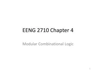
4.1 Device Structure and Physical Operation (Physical structure of the enhancement-type NMOS transistor) cross-section perspective view Typically L = 0.1 to 3 mm, W = 0.2 to 100 mm, and the thickness of the oxide layer (tox) is in the range of 2 to 50 nm.
4.1 Device Structure and Physical Operation • 4.1.1 Device Structure • Source (S) connects to Body (B), Drain (D) is at a positive voltage relative to S, two pn junctions are cut off • Substrate: no effect on device operation →3 terminals device • Source and drain can be interchanged
4.1.4 Applying a Small VDS An NMOS transistor with vGS (gate voltage) > Vt (threshold voltage)and with a small vDS applied. The device acts as a resistance whose value is determined by vGS. Specifically, the channel conductance is proportional to vGS – Vt’ and thus iD is proportional to (vGS – Vt) vDS. Note that the depletion region is not shown (for simplicity).
4.1.4 Applying a Small VDS (Cont.) The iD (drain current) – vDS (drain voltage) characteristics of the MOSFET in the above slide when the voltage applied between drain and source, vDS, (drain source) is kept small. The device operates as a linear resistor whose value is controlled by vGS(gate source).
4.1.5 Operation as VDS Is Increased Operation of the enhancement NMOS transistor as vDSis increased. The induced channel acquires a tapered shape, and its resistance increases as vDS is increased. Here, vGS is kept constant at a value > Vt.
4.1.6 Derivation of the ID –VDS relationship The drain current iD versus the drain-to-source voltage vDS for an enhancement-type NMOS transistor operated with vGS> Vt.
4.1.8 Complementary MOS or CMOS Cross-section of a CMOS integrated circuit. Note that the PMOS transistor is formed in a separate n-type region, known as an n well. Another arrangement is also possible in which an n-type body is used and the n device is formed in a p well.
4.2 Current-Voltage Characteristics4.2.1 Circuit Symbol (a) Circuit symbol for the n-channel enhancement-type MOSFET. (b) Modified circuit symbol with an arrowhead on the source terminal to distinguish it from the drain and to indicate device polarity (i.e., n channel). (c) Simplified circuit symbol to be used when the source is connected to the body or when the effect of the body on device operation is unimportant.
4.2.2 The ID –vDS Characteristics • There are three distinct regions of operation: • The cut-off region • The triode region • The saturation region
4.2.2 The ID –vDS Characteristics (Cont.) (a) An n-channel enhancement-type MOSFET with vGS and vDS applied and with the normal directions of current flow indicated. (b) The iD–vDS characteristics for a device with k’n(W/L) = 1.0 mA/V2.
4.2.2 The ID –vDS Characteristics (Cont.) The N-channel enhancement-type MOSFET Operates in the triode region when vGS is greater than Vi and the drain voltage is lower than the gate voltage by at least Vt .
Problem 4.7c&d (Cont.) ox for silicon = 3.45x10⁻¹¹
4.2.2 The ID –vDS Characteristics (Cont.) The N-channel enhancement-type MOSFET Operates in the saturation region when vGS is greater than Vi and the drain voltage does not fall below the gate voltage by more than Vt .
4.2.2 The ID –vDS Characteristics (Cont.) The iD–vGS characteristic for an enhancement-type NMOS transistor in saturation (Vt = 1 V, k’nW/L = 1.0 mA/V2).
4.2.2 The ID –vDS Characteristics (Cont.) Large-signal equivalent-circuit model of an n-channel MOSFET operating in the saturation region
4.2.3 Finite Output Resistance in Saturation Increasing vDS beyond vDSsatcauses the channel pinch-off point to move slightly away from the drain, thus reducing the effective channel length (by L).
4.2.3 Finite Output Resistance in Saturation Eq. 4.22 Eq. 4.24 Large-signal equivalent circuit model of the n-channel MOSFET in saturation, incorporating the output resistance ro. The output resistance models the linear dependence of iD on vDSand is given by Eq. (4.22).
Another Design Example Figure 1
Another Design Example Assume saturation Figure 2
Figure (c) Assume saturation ID = 2 = (½)(1)(Vov)2) (Vov)2 = 4 Vov = 2 , However, Vov = -2 V since pmos circuit VGS = Vt + Vov = -2 -2 = - 4 Thus Vs = 4 V = V4 V5 = -10 - ( - (2.5x10³)(2x10⁻³)) = - 10 + 5 = -5 V
Figure (d) ID = 2 = (½)(1)(Vov)2) (Vov)2 = 4 Vov = 2 , However, Vov = -2 V since pmos circuit VGS = Vt + Vov = -2 -2 = - 4 , Vs = 4 V6 = 10 – 4 = 6 V V7 = 6 – 4 = 2 V
4.4.1 Large-signal Operation –The Transfer Characteristic • Common Source Amplifier (CS) • To determine the voltage transfer • characteristic between vI and vO • VI = vGS • VO = vDS = VDD - RDiD • Graphically and analytically Basic structure of the common-source amplifier Graphical construction to determine the transfer characteristic of the amplifier in (a).
4.4.2 Graphical Derivation of the Transfer Characteristic Transfer characteristic showing operation as an amplifier biased at point Q.
4.4.4 Operation as a Linear Amplifier Two load lines and corresponding bias points. Bias point Q1 does not leave sufficient room for positive signal swing at the drain (too close to VDD). Bias point Q2 is too close to the boundary of the triode region and might not allow for sufficient negative signal swing.
4.4.5 Analytical Expressions for the Transfer Characteristic Cutoff-Region Segment, XA
4.4.5 Analytical Expressions for the Transfer Characteristic (Cont.) Av = - 2 (VDD – VOQ) / VOV = - (2VRD) / VOV
Example (Cont.) Av = - 2 (VDD – VOQ) / VOV = - (2VRD) / VOV
4.4.5 Analytical Expressions for the Transfer Characteristic (Cont.)