Download
1 / 12
610 likes | 2.45k Vues
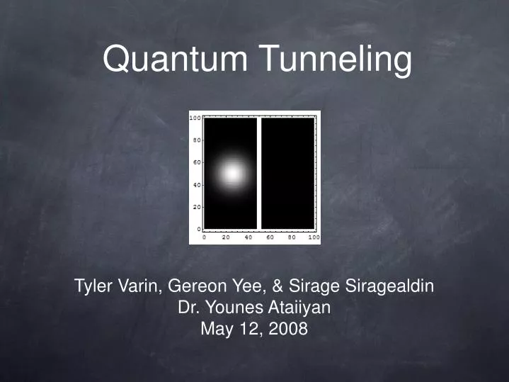
Quantum Tunneling. Tyler Varin, Gereon Yee, & Sirage Siragealdin Dr. Younes Ataiiyan May 12, 2008. History of Quantum Tunneling. Consequence of the wave nature of matter First used to explain alpha decay of heavier elements in 1928 by George Gamow

E N D
Quantum Tunneling • Tyler Varin, Gereon Yee, & Sirage Siragealdin • Dr. Younes Ataiiyan • May 12, 2008
History of Quantum Tunneling • Consequence of the wave nature of matter • First used to explain alpha decay of heavier elements in 1928 by George Gamow • Shown experimentally by Leona Esaki in 1958 in the tunneling diode
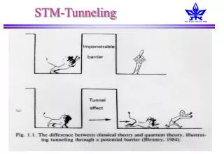
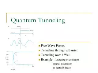
What is Quantum Tunneling? • At the quantum level, matter has corpuscular and wave-like properties • Tunneling can only be explained by the wave nature of matter as described by quantum mechanics • Classically, when a particle is incident on a barrier of greater energy than the particle, reflection occurs • When described as a wave, the particle has a probability of existing within the barrier region, and even on the other side of it
How Can This Be? • Solutions to the wave equation have the general form (I) • In the barrier region, the solution becomes (II) • The wave function decays exponetially in the barrier region • If some portion of the wavefunction still exists on the other side of the barrier, transmission has occurred • The width of the barrier is the most prominent factor in determining the probability of transmission (I) (II) Images courtesy of Wikipedia
Wave Packet Demonstration • University of Colorado Tunneling Program • From http://phet.colorado.edu/new/simulations/sims.php?sim=Quantum_Tunneling_and_Wave_Packets
Tunneling & α-Decay • George Gamow used tunneling to explain α-decay in Uranium 238 • The α particle does not have enough kinetic energy to escape the nucleus • There is a chance, due to it’s wave function, that it will escape the potential barrier of the nucleus boundary • Due to the exponential decay nature of the wave function in the barrier region, the width of the barrier can manifest itself in the half-life of the isotope
Tunneling & Microchip Development • As microchip developers create smaller production processes, we reach the limit of classical computer technology • The feature size of the most advanced microchip today is 45 nm • With such small widths, the electrons in the channel can tunnel out with relative ease, possibly affecting other transistors in the chip • Current approximations show that the minimum feature size is about 4 nm • After that point tunneling is not only possible, but highly likely and the chip would fail
Scanning Tunneling Microscopes • The Scanning Tunneling Microscope was invented in 1981 by Gerd Binnig and Heinrich Rohrer • When a metal tip, usually made of tungsten or platinum-iridium, is brought within .4-.7nm of the sample, electrons tunnel across the gap and create a current in the tip • This current is then fed to a computer and used to generate an image of the atomic surface of the sample Image courtesy of Wikipedia
At this distance the coulomb force between the tip and an atom of the sample is actually enough to move the atom • This has allowed physicists to create images and structures on the atomic level Images courtesy of IBM
Tunneling Diodes • Developed in 1958 by Leona Esaki at Sony • Tunneling diodes are designed with a heavily doped p-n junction that is only 10 nm wide • At low voltages, the p and n states are aligned, allowing electrons to tunnel across the gap • As voltage increases these states become more misaligned and fewer electrons flow • This negative resistance region allows the diode to operate at very high frequencies, well into the Gigahertz range Image courtesy of Wikipedia
Force Sensors • A UK company is developing flexible force sensors that use quantum tunneling • These sensors are made out of Quantum Tunneling Composite materials • QTC’s are essential non-conducting in their normal state • When flexed by an applied force, the atoms of the QTC are brought close enough so that tunneling can occur • Tunneling changes the QTC from an insulator to a conductor with a predictable exponential decay in resistance Image courtesy of Peratech
Works Cited • http://www.peratech.co.uk/science.htm • http://en.wikipedia.org/wiki/Tunnel_diode • http://en.wikipedia.org/wiki/Quantum_tunneling • http://en.wikipedia.org/wiki/Scanning_tunneling_microscope • http://psi.phys.wits.ac.za/teaching/Connell/phys284/2005/lecture-02/lecture_02/node13.html • Rex, A. & Thornton, S. T. (2006) Modern Physics for Scientists and Engineers 3rd ed. Belmont CA: Thomson Brooks/Cole • http://www.almaden.ibm.com/vis/stm/gallery.html