Download
1 / 37
460 likes | 1.1k Vues
Unit 1.1 :. Basic MOS Technology. ( Pucknell p:-1-24) . Moore’s law. Levels of Integration:-. i ) Small Scale Integration:- ( 10-100 ) transistors => Example: Logic gates ii) Medium Scale Integration:- ( 100-1000 ) => Example: counters iii) Large Scale Integration:- ( 1000-20000 ) =>

E N D
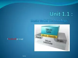
Unit 1.1 : Basic MOS Technology (Pucknell p:-1-24) ECEA
Moore’s law ECEA
Levels of Integration:- i) Small Scale Integration:- (10-100) transistors => Example: Logic gates ii) Medium Scale Integration:- (100-1000) => Example: counters iii) Large Scale Integration:- (1000-20000) => Example:8-bit chip iv) Very Large Scale Integration:- (20000-1000000) => Example:16 & 32 bit up v) Ultra Large Scale Integration:- (1000000-10000000) => Example: Special processors, virtual reality machines, smart sensors ECEA
Basic MOS Transistors • We have PMOS and NMOS transistors. • They are Enhancement mode and Depletion mode of operation ECEA
In Enhancement mode transistor channel is going to form after giving a proper gate voltage. ECEA
In Depletion mode transistor channel will be present by the implant. It can be removed by giving a proper negative gate voltage. ECEA
Enhancement mode Transistor action:- • Cutoff :Gate voltage(Vgs) is less than threshold voltage (Vt) at Drain voltage(Vds)=0v. ECEA
This region is called the non-saturation Region or linear region : the drain current(Ids) increases linearly with Vds and the channel starts to narrow on drain side. ECEA
Saturation Region: the drain current remains almost constant. (As the drain voltage is increased further beyond (Vgs-Vt) the pinch off point starts to move from the drain end to the source end) ECEA
Depletion mode Transistor action:- • Channel is established due to the implant even when Vgs = 0 and the channel can be cut off by applying a negative voltage between the gate and source. ECEA
n-MOS fabrication process • Process is carried out on a thin wafer (75 to 150 mm dia, .4mm thick) • Doped with boron impurity concentration of 1015/cm3 to make substrate Substrate ECEA
n-MOS fabrication process 2) A layer of SiO2 grown all over the surface (1µm thick) to protect. SiO2 Substrate ECEA
Photolithography 3) Then the oxidized wafer is covered with Photo resist. Photo-Resist SiO2 Substrate ECEA
Photo-Mask Photolithography 4) Now the wafer is exposed to UV Light through a photo mask to define regions. Photo-Resist SiO2 Substrate ECEA
Photolithography 5.1) Now oxide which is unprotected from photoresist is etched away. SiO2 Substrate ECEA
Photolithography 5.2) The rest of the photo resist is removed. Then the further fabrication process is carried out, say doping. SiO2 SiO2 Substrate ECEA
Thin layer of SiO2(0.1µm) grown and then polysilicon is deposited on top to form gate structur. Polysilicon layer consists of heavily doped polysilicondepositd by CVD. Polysilicon on thin oxid Poly Si SiO2 Thinox Substrate ECEA
Metallization 7) Use mask to remove exposed area into which n-type impurities(phosphorus) are to be diffused to form source and drain. n n SiO2 Poly Si Thinox Substrate ECEA
Metallization 8) Again thinox is grown all over the surface and is then masked to expose selected areas of gate, drain and source to make Contact holes (cut) n n Poly Si SiO2 Thinox Substrate ECEA
Metallization 9) Finally, whole chip is metal deposited over its surface for required interconnection pattern. n n Poly Si SiO2 Thinox Substrate ECEA
CMOS fabrication • When we need to fabricate both nMOS and pMOStransistors on the same substrate we need to follow different processes. • The three different processes are , P-well process ,N-well process and Twin tub process. ECEA
P-well process • Mask sequence. • Mask 1: Defines the areas in which the deep p-well diffusion takes place. • Mask 2: Defines the thin oxide region (where the thick oxide is to be removed or stripped and thin oxide grown) • Mask 3: It’s used to pattern the polysilicon layer which is deposited after thin oxide. ECEA
Mask 4: A p+ mask (anded with mask 2) to define areas where p-diffusion is to take place. • Mask 5: We are using the –ve form of mask 4 (p+ mask) It defines where n-diffusion is to take place. ECEA
Mask 6: Contact cuts are defined using this mask. • Mask 7: The metal layer pattern is defined by this mask. • Mask 8: An overall passivation (overglass) is now applied and it also defines openings for accessing pads. ECEA
Define nMOS and pMOS active areas Field and gate oxidations (thinox) Form and pattern polysilicon p+ diffusion n+ diffusion Contact cuts Deposit and pattern metallization Over glass with cuts for bonding pads Formation of n-well regions Main step in a typical n-well process ECEA
n-Well CMOS ECEA
Twin-tub COMS • n-type material and then we create both n-well and p-well region. ECEA
Bi-CMOS • Driving capability of MOS transistors is less • Bi-Cmos technology capable to drive large capacitive loads. ECEA
Bi-CMOS The npn transistor is formed an n-well & the additional p+ base region is located in the well to form the p-base region of the transistor. The second additional layer, the buriedn+subcollector(BCCD) is added to reduce the n-well (collector) resistance & thus improve the quality of the bipolar transistor. ECEA
Comparison between CMOS and Bipolar technologies CMOS Bipolar technologies • Low static power dissipation • High input impedance • Scalable threshold voltage • High noise margin • High packing density • High delay sensitivity to load • Low output drive current • Low gm • Bidirectional capability • A near ideal switching device • High power dissipation • Low input impedance • Low voltage swing logic • Low packing density • Low delay sensitivity to load • High output drive current • High gm • Essentially unidirectional ECEA
cost versus delay graph • CMOS for logic • BiCMOS for I/O • ECL for critical high speed parts ECEA
Production of e-beam masks: • The steps in production of e-beam masks. • Starting materials is chromium coated glass plates which are coated with e-beam sensitive resist. • E-beam machine is loaded with the mask description data. • Plates are loaded into e-beam machine, where they are exposed with the patterns specified by mask description data. ECEA
After exposure to e-beam, plates are introduced into developer to bring out patterns. • The cycle is followed by a bake cycle which removes resist residue. • The chrome is then etched and plate is stripped of the remaining e-beam resist. ECEA
Their are two types of scanning, Raster scanning and vector scanning to map the pattern on to the mask. • In raster type, e-beam scans all possible locations and a bit map is used to turn the ebeam on and off, depending on whether the particular location being scanned is to be exposed or not. • In vector type, beam is directed only to those location which are to be exposed. ECEA
Advantages e-beam masks: • Tighter layer to layer registration; • Small feature sizes ECEA