Download
1 / 15
150 likes | 306 Vues
Three dimensional patterned MgO substrates ~ fabrication of FZO nanowire structure~. Tanaka Lab. Yasushi F ujiwara. Contents. Introduction of k eyword 3d transition metal oxide & FZO Magnetic domain and magnetic domain wall Constricted ferromagnetic nanowire structure

E N D
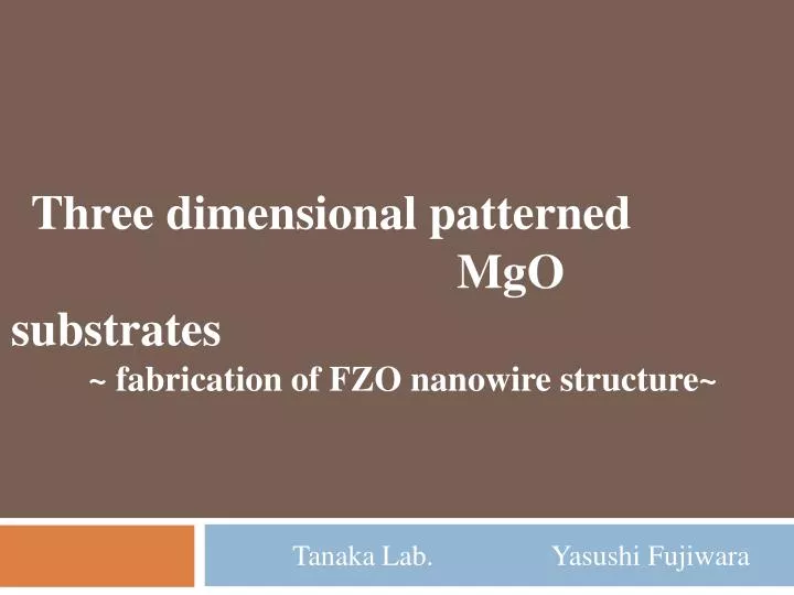
Three dimensional patterned MgO substrates ~ fabrication of FZO nanowire structure~ Tanaka Lab. Yasushi Fujiwara
Contents • Introduction of keyword • 3d transition metal oxide & FZO • Magnetic domain and magnetic domain wall • Constricted ferromagnetic nanowire structure • Nano processing procedure for metal oxides • My research • Sidewall growth method & Fabrication process • Anneal condition • Three dimension MgOnanowire structure • Structure analysis by TEM • MgO growth mechanism • Conclusion
Contents • Introduction of keyword • 3d transition metal oxide & FZO • Magnetic domain and magnetic domain wall • Constricted ferromagnetic nanowire structure • Nano processing procedure for metal oxides • My research • Sidewall growth method & Fabrication process • Anneal condition • Three dimension MgOnanowire structure • Structure analysis by TEM • MgO growth mechanism • Conclusion
Fe Al O Si 3d transition metal oxide(3d遷移金属酸化物) Strongly-correlated electron systemVariety of function Spinel structure (強相関電子系) Fe3+ Control of carrier concentrate Fe3-xZnxO4(FZO) Ti O2- Fe2+ V PRB. 76 205108(2007) Cr Ferromagnetic at roomtemperature and high spin polarization High temperature superconduction YBa2Cu3O7 Ferroelectric BaTiO3 Ferromagnetic Fe3O4,Fe3-xZnxO4 Metal-Insulator transition VO2 Mn Enviromental friendly material (環境調和型材料) Zn Fe Clark number O : (49.5) 1 Fe : (4.70)4 Co O PRB. 76 205108(2007) Fe science 303 661(2004) Thin solid films 486 46(2005) small4 1661(2008) PRL.581574(1987) Ni Cu
Ferromagnetic nanostructures Pinning domain wall Magnetic domain ➞Field of one direction of magnetic moment Magnetic Domain wall ➞Field of rotation spin among magnetic domain (磁区) (磁壁) Merit Magnitic domain wall • Nonvolatile • High speed • High integration • Low consumed power • Unlimitedlywrite • Unlimitedly read Fe3-xMnxO4-nanowire MFM image Magnetic domain Magnetic domain Applied Physics Express 4 (2011) 033001 application 50nm NanoLett. 9 1962(2009) Current-driven domain wall motion in a magnetic constricted nanowire Nonconventional giant nonlinearly response 100nm ~50nm ~70nm Average of non-uniform magnetic 応用物理 79 1071(2010)
Nano processing procedure for metal oxides Oxide has high physical hardness and chemical stability. It is diffcult to fabricate a few dozen nanometer patterns. Bottom up Top down Photo lithography FIB lithography Pulse laser deposition chemical vapor deposition LaAlO3 ZnO ZnO Cu2O3 APL. 84 5213(2004) APL. 89 122101(2006) EB lithography AFM lithography MoO3 TiO2 NanoLett. 9 1962(2009) Appl. Surf. Sci. 253 1758(2006) SuperlatticeMicrost46 513(2009) JJAP. 42 6721(2003)
Contents • Introduction of keyword • 3d transition metal oxide & FZO • Magnetic domain and magnetic domain wall • Constricted ferromagnetic nanowire structure • Nano processing procedure for metal oxides • My research • Sidewall growth method & Fabrication process • Anneal condition • Three dimension MgOnanowire structure • Structure analysis by TEM • MgO growth mechanism • Conclusion
Combination method Nanoimprint(NIL) • High processing accuracy of side surface • Control of position and shape Pulse laser deposition(PLD) • Deposition of thin film from atomic layer • The most suitable method to fabricate thin film of oxide • Deposition time and angle ➞Control of width • Shape of substrate • ➞Control of shape and height of oxide structure Excimer laser ~10nm substrate Fabrication of highly ordered nanopattern structures
Purpose substrate substrate Fabrication of highly ordered nanowire structures • Anneal condition of MgOcrystalization • Structure analysis by TEM • MgOnanowire growth mechanism
Fabrication process Three dimension MgOnanowire MgO resist MgOsubstrate MgOsubstrate MgOsubstrate MgOsubstrate ①cleaning substrate ②nanoimprint ③PLD(MgO) ④removing resist FZOnanowire FZO <a few dozen nm MgOsubstrate MgOsubstrate ⑦removing MgO ⑥PLD(FZO)&ECR ⑤annealing MgOsubstrate
MgO crystallization condition by postanneal MgO STO(003) STO(002) MgO(022) STOsubstrate STOsubstrate • MgO was crystallized by postannealing at 1000℃
[010] [010] [010] [010] [010] [010] Anisotropy growth of MgOnanowire [100] [100] [100] [100] [100] [100] MgOnanowire Schematic diagram After anneal (1000℃) Before anneal MgOnanowire MgO(001)nanowire substrate Zig-Zag line MgOsubstrate [001] MgO(001)substrate MgO(001)substrate [001] 300nm [001] 500nm MgOnanowire MgO(001)nanowire MgOnanowire Parallel line 300nm [010] MgO(001)substrate MgO(001)substrate 500nm [100] [001] [001] MgOsubstrate [001]
Structure analysis of MgOnanowire (TEM) MgOnanowire(TEM) MgOnanowire(FFT) MgOnanowire MgOsubstrate 2nm 200nm Fracture direction MgO substrate(TEM) MgOsubstrate(FFT) MgOnanowire [110] MgOsubstrate 10nm I confirmed that quality of crystallized MgOnanowires is similar to MgO substrates.MgO grows so that MgOnanowire(001)[100]//MgOsubstrate(001)[100]. 2nm
[010] [010] [010] [010] [010] MgO growth mechanism [100] [100] [100] [100] [100] MgOnanowire MgO(001)nanowire substrate Zig-Zag line [110] MgO(001)substrate [001] [001] Growth mechanism MgO(001)nanowire MgOnanowire Flatness line 500nm [110] MgO(001)substrate 500nm [001] [001] I confirmed that MgO(110)appears in side surface of MgOnanowire.
Conclusion • I tried to fabricate the three dimension MgOnanowire structures. • I confirmed that MgO was crystallized by postannealing at 1000℃. • I confirmed that quality of crystallized MgOnanowires is similar to MgO substrates. • I confirmed MgO growth mechanism by TEM. • I succeed in fabrication of the MgOnanowires structure with flat MgO(110) side surface. • I have been trying to fabricate FZO nanowire structures on the 3D MgOnanowire substrate, and study their magnetic properties. Future plane