Download
1 / 54
750 likes | 1.41k Vues
Nanoimprint lithography (NIL). Overview. Thermal NIL resists. Residual layer after NIL. NIL for large features (more difficult than small one). Room temperature NIL, reverse NIL, NIL of bulk resist (polymer sheet, pellets).

E N D
Nanoimprint lithography (NIL) Overview. Thermal NIL resists. Residual layer after NIL. NIL for large features (more difficult than small one). Room temperature NIL, reverse NIL, NIL of bulk resist (polymer sheet, pellets). ECE 730: Fabrication in the nanoscale: principles, technology and applications Instructor: Bo Cui, ECE, University of Waterloo; http://ece.uwaterloo.ca/~bcui/ Textbook: Nanofabrication: principles, capabilities and limits, by Zheng Cui
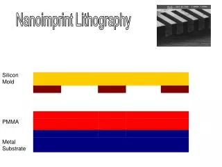
Nanoimprint lithography: patterning by mechanical replication mold substrate
Two NIL approaches Thermal NIL UV-curing NIL UV-light RIE residual layer, transfer into under-layer RIE residual layer Heat up to soften the resist, imprint, cool down and separate Liquid (soft) resist, hardened by UV irradiation due to cross-linking
Thermal nanoimprint Temperature and pressure evolution during thermal press nano-imprinting Temperature Pressure • Typical temperature is 100oC – 200oC, 30-50oC above resist’s glass transition temperature. • Typical pressure is about 20-50 atm, depends on resolution and pattern in the mold (easy for protruded feature, higher pressure for recessed feature in mold)
Printing: some history During 1041-1048, Bi Sheng invented movable type printing technique. Hardened clay as mold. 12th century metal type printing techniques were developed in Korea. 1450 Gutenberg introduced his press. 300 two-volume bibles printed. ……… 1970´s compact disks (CD). 1996, Nano-Imprint Lithography (NIL), sub-10 nm feature size, high throughput and low cost. Today, NIL is one candidate (though not top candidate) for next-generation lithography for IC industry. The bottom line is, NIL has the highest resolution (sub-5nm) and is fast. It will come into play when no other lithography can do the job. Duplicated by NIL (2000) Gutenberg bible (1450)
NIL not ready yet for ICs, but never excluded ML2: maskless lithography (EBL, SPM..) ITRS (2006) Projections for Lithography Technology
Key advantage of NIL: highest resolution Sub-5 nm features and 14nm pitch nanoimprint Yet, feature size and pitch still limited by mold making. They can go smaller. No more light diffraction limit, charged particles scattering, proximity effect… Sub-10nm feature size, over a large area with high throughput and low cost.
Another key advantage: 3D imprinting • Patterning of the via and interconnect layers simultaneously, in CMOS BEOL . • Thus potentially reduces the number of masking levels needed in BEOL. • (BEOL: back end of line) 3D mold Wikipedia: Back end of line (BEOL) is the portion of integrated circuit fabrication line where the active components (transistors, resistors, etc.) are interconnected with wiring on the wafer. BEOL generally begins when the first layer of metal is deposited on the wafer. It includes contacts, insulator, metal levels, and bonding sites for chip-to-package connections.
Imprinting in presence of a dust particle Dust is one of the most serious problems for NIL, defect area>>dust size. To prevent mold wafer breaking, sandwich the mold/substrate stack with something soft, such as a paper or plastic.
Nanoimprint lithography (NIL) Overview. Thermal NIL resists. Residual layer after NIL. NIL for large features (more difficult than small one). Room temperature NIL, reverse NIL, NIL of bulk resist (polymer sheet, pellets).
Desired resist properties • Good adhesion to the substrate, uniform film thickness, easy spinning. • High pattern transfer fidelity, no adhesion to the mold during separation. • Low viscosity during imprinting. • Low imprint pressure and temperature. • But sufficient thermal stability in subsequent processes, e.g. RIE, lift-off. • High plasma etch resistance for pattern transfer into under-layers. • Soluble in non-toxic solvents, for spin-coating. • Minimal shrinkage (for UV and thermal curable resist). • Mechanical strength and tear resistance.
How much initial material (resist) is needed? • Polymer is not compressible, so conservation of volume. • Too thick h0 leads to large hf, difficult for pattern transfer. • Too thin h0 increases mold wear and damage. Alternative Lithography: Unleashing the Potentials of Nanotechnology (book), 2003.
“Standard” resist for NIL: PMMA Glass transition and flow temperature of PMMA TS: sub-transition TG: glass transition TF: flow (In principle, NIL can be done at just slightly above Tg) However, PMMA is far away from being an ideal NIL resist. It is popular simply because people are familiar with it (since it is resist for many other lithographies).
Shear modulus of different molecular weight PMMAs Flow temperature of PMMA (and other amorphous polymers) increases with increasing molecular weight. Unit for Mw: g/mol Comments: PMMA is the choice for beginners, not optimized for NIL. Tg=105oC, NIL at >150oC. Polystyrene (Tg close to PMMA) is slightly better – easy separation due to lower surface energy. Poly(vinyl phenyl ketone) is comparable to polystyrene but with Tg only 58oC. NIL at 95oC.
Another thermal NIL resist: TOPAS polymers TOPAS: Cyclic olefinic copolymer (norbornene and ethylene) Attractive properties: – very un-polar – very low water absorption – high optical transparency (>300 nm) – high chemical resistance – low surface energy – high plasma etch resistance But finding solvent system giving homogeneous and stable solutions is not an easy task (chemical resistance, hard to dissolve) Applications: lab-on-a-chip micro-fluidic system… Commercial TOPAS solutions: (from Micro-Resist) mr-I T85 with Topas grade 8007 mr-I T65 with Topas grade 9506 Similar product: Zeonor from Zeon or Zeonex
plasticizer Plasticizer: monomers, solvents, small molecules no plasticizer + plasticizer + lots plasticizer Plasticizer: decreased chain entanglement, increased chain motion Tg can be lowered by adding plasticizer into the resist
Polymer with low Tg • Low imprint temperature • Good polymer flow at moderate temperature • Less problems with thermal expansion • Shorter thermal cycle time Example: thermoplastic with Tg 40 °C Left: 400 nm lines and trenches: immediately after imprinting Right: same patterns after heating the imprint to 60°C for 5min. • Thermal stability of imprinted patterns (deterioration by thermal flow) is determined by the glass transition temperature. • Sufficient thermal stability of imprinted patterns is necessary in subsequent processes such as metal evaporation for liftoff or plasma etching.
If Tg is too low… 10 days after imprinting a low Tg resist
Approach to thermal stability Thermal-set/curable resist: (low Tg pre-)polymer is cured (cross-linked) upon heating, making it stable at very high temperatures.
Thermal and photochemical curing Cured polymer Linear or branched thermoplastic (pre)polymer Thermal curing is also called “thermal set” Curing: Cross-linking of the macromolecules, generation of a spatial macromolecular network.
Fast iso-thermal (no thermal cycle, no cooling) nanoimprint • Isothermal imprinting due to increase in Tg during imprinting (so no need to cool down). • Reduce issues of thermal expansion. • Decrease considerably imprint time (since no cooling). Film thickness 170nm, 100nm trenches, 10-20nm residual layer. Add initiator + plasticizer: Imprint at 100oC for 10min, no cooling. (Initiator to increase curing speed; plasticizer to lower imprint temperature) Starting model system: NIL at 190oC for 1 hour for sufficient curing.
Functional resist: nano-crystal (NC)/polymer based materials • Synthesis and functionalisation of colloidal nano-particles for incorporation into thermoplastic or thermal-curing (i.e. thermal-set) polymers. • Tuning of functional properties: • Optical absorption and emission • Mechanical Stability • Conductivity • Processability… Size dependent luminescent CdSeNCs (quantum dot) http://en.wikipedia.org/wiki/Cadmium_selenide
Imprinting on luminescent nano-crystal/PMMA based co-polymer composites No illumination Under illumination CdSe@ZnS nano-crystals (NC) in PMMA modified co-polymer. Homogeneous distribution of NCs inside the polymer matrix.
1 m Functional “resist”: semiconducting polymer SEM image of 200nm period MEH-PPV grating R-P3HT grating with 200nm period MEH-PPV Tg=65oC. Hot embossing at 120oC and 20bar. MEH-PPV spun on a PEDOT/ITO/glass. R-P3HT 200nm period grating. NIL at 160oC and 35 bar. Strong physical bond, high transition temperature.
Metal electrode Glass N ITO P P N ITO Transparent substrate Al Application: nanostructured plastic solar cell MEH-PPV is a popular p-type semiconducting polymer for plastic solar cell. (The n-type material is Alq3, http://en.wikipedia.org/wiki/Tris(8-hydroxyquinolinato)aluminium) Classic planar p-n junction, low junction area, low efficiency Nanostructured junction, high junction area, high efficiency • Plastic solar cells: flexible, light weight, tunable electrical properties, and potential lower fabrication cost. • Limitation: low energy conversion efficiency due to low carrier mobility. • Method to increase efficiency: increase the interface area by nano-patterning the p-n junction.
Nanoimprint lithography (NIL) Overview. Thermal NIL resists. Residual layer after NIL. NIL for large features (more difficult than small one). Room temperature NIL, reverse NIL, NIL of bulk resist (polymer sheet, pellets).
Residual layer: thinner is better for easier pattern transfer Resist Substrate Residual layer HR is too thick RIE Too thick residual layer makes subsequent RIE more demanding: hard to control profile, pattern size shrinkage (CD loss). So resist thickness should be pattern height of mold. CD: critical dimension. Such a tapered profile makes liftoff almost impossible
How to get rid of residual layer (thermal NIL aided by UV exposure) Add light-blocking metal layer (here Ni), and use resist developer instead of O2 RIE to remove the residual layer. Comparison of residual layers in micro-scale resist pattern obtained by: (a) conventional NIL; (b) the current technique where no residual layer is left. Un-exposed area developed (since SU-8 is negative resist) Cheng and Guo, “A combined-nanoimprint-and-photolithography patterning technique”, MEE, 2004.
ICP etching of residue layer ICP: inductively coupled plasma, high plasma density and etching rate, better control • (According to an ICP tool seller, usually very difficult to get such etching result) • ICP provides the best performance for etching residual layer: • Low pressure processing minimizes isotropic (lateral) etching and loss of profile. • Lower temperature processing also helps. • Low bias processing minimizes faceting at the top of the lines. Polystyrene residue removal on Al. 200nm residual removed in 2 minutes using a pure O2 ICP plasma – linewidth remains constant at 0.35μm (??) and sidewall is vertical.
Nanoimprint lithography (NIL) Overview. Thermal NIL resists. Residual layer after NIL. NIL for large features (more difficult than small one). Room temperature NIL, reverse NIL, NIL of bulk resist (polymer sheet, pellets).
UV-curable NIL, 2nm carbon nanotube mold NIL for smallfeatures/high resolution (<10nm) Press liquid into a nano-hole Pressure (P) F=2R Surface tension () Pressure 1/diameter. But for protruded mold features (pillars…), local pressure at the pillar is much higher than average - easy to imprint. Hua … Rogers, “Polymer imprint lithography with molecular-scale resolution”, Nano Lett. 2004
NIL for large features (>100 m) - simultaneous pattern duplication of large and small features • Application: large features are needed to connect small ones to the outside world (electrodes…). • Challenge: more polymer must be displaced over longer distances. • A popular approach: two-step process - small features by NIL, large ones by photolithography with alignment. Problems when both small and large features are present Schematics of pattern failure mechanisms in NIL as a result of: (a) non-uniform pattern height; (b) non-uniform residual layer thickness; (c) incomplete nano-pattern replication. Cheng, “One-step lithography for various size patterns with a hybrid mask-mold”, Microelectronic Engineering 71, 288–293 (2004).
NIL pattern uniformity Etch some dummy holes/trenches here • Different “fill factors” across mold lead to different sinking rates. • Mold bending leads to non-uniform residual layer on substrate. • One solution: fabricate “dummy” cavities/protrusions to create constant fill factor.
Combined photo- (for macro) and nanoimprint lithography (for nano) hybrid mask-mold SU-8 Here SU-8 is used both as a photo-resist and thermal NIL resist. (SU-8 is a photo-resist, but not a UV-curing NIL resist as it is hard to imprint at room temperature. Instead, it can be used as a thermal NIL resist, Tg50oC) UV exposure Using a hybrid mask-mold for one-step lithography of both large- and nano-patterns After development SEM micrograph of resist patterns obtained by the technique with hybrid mask-mold. Cheng, “One-step lithography for various size patterns with a hybrid mask-mold”, Microelectronic Engineering 71, 288–293 (2004).
L L L mold h0 h0 Liquid Substrate Modeling of liquid flow for large features (>>pattern depth) y x • Assumptions: • Periodic mold structure (period 2L) • Ignore inertial, gravitational force and surface tension • Resist film thickness = mold trench depth = h0 L: achievable feature size p: pressure : imprinting time : viscosity h0: film thickness
Derivation of the equation For fully-developed laminar flow between infinite parallel plates, the velocity is given by (u=0 at y=0, h) where is viscosity and p/x is pressure gradient along the x direction. Ignoring z-dimension, then the volumetric flow-rate is (average velocity times h) But on the other hand the volume of the liquid changes at a rate Solving for h we get If assume h=h0/2 at t= and assuming p/x=2P/(L/2) (the factor 2 in front accounts for the fact that the actual contact area is only half the mold area), we obtain the critical pattern size
Strategy to imprint large features (mm) For thermoplastic polymer PMMA at T>Tg Mw: molecular weight n=1 for Mw<MC, un-entangled molecules n=3.4 for Mw>MC, entangled molecules Viscosity of 110 kg/mol PMMA vs. temperature Viscosity for PMMA (Mc=30kg/mol) a) 12 kg/mol, 200oC; b) 12 kg/mol,150oC; c) 120 kg/mol, 200oC a:b:c=1:126:278 Therefore, use low molecular weight PMMA and imprint at high temperature
But for nanoscale features… after excessive etch Such a profile makes liftoff difficult. Solution: use tri-layer resist system Problems of imprinting simultaneously large (mm) and small (nm) features Square (mm) imprinted into PMMA Optical image Profile 200nm 2mm Schematic mold wafer Bended mold Tri-layer resist resist need to etch PMMA silicon wafer PMMA thin SiO2 Due to mold bending, need excessive etch to remove the thick residual resist at the square center bottom polymer layer
Fabrication process flow Mold Nano feature Large feature Tri-layer resist PMMA 4. RIE ARC (O2 gas, etch little SiO2) SiO2 ARC Cr silicon wafer 1. Imprint ARC: Anti-reflection coating, cross-linked polymer. 5. Evaporate Cr 2. RIE PMMA (excessive etch) 6. Liftoff Cr (dissolve ARC) 7. RIE Si (etch little Cr) 3. RIE SiO2 (CHF3 gas)
Result of simultaneous imprinting large and small features 1.6mm square Line-width in the mold is 80nm Line-width in the duplicated pattern is 98nm 50 40 30 98nm 1.3mm square Line-width change (nm) 20 10 0 90 120 150 180 210 240 270 PMMA etched (nm) (RIE PMMA 180nm) Summary: For small features, line-width increased by 18nm. For large features, 1.3mm squares were faithfully duplicated. Cui and Veres, “Pattern replication of 100 nm to millimeter-scale features by thermal nanoimprint lithography”, MEE, 2006
NIL of high aspect ratio structures • Low molecular weight (Mw) has low viscosity, so is easy to imprint. • But it also has low shear modulus, which makes the pattern easily broken during separation if the pattern is of high aspect ratio. • The solution is a double-layer resist stack, bottom layer high Mw for its strength (not easily broken) and top layer low Mw for its good flow capability. High-aspect-ratio pattern imprinted using double-layered polymer process. Top layer: PMMA (Mw=15kg/mol), 0.7m; base layer: PMMA (996kg/mol), 1.5m. 170oC, 150bars, 250nm lines; pattern height: 1.3m. Schematic of double-layer nano-imprinting
Nanoimprint lithography (NIL) Overview. Thermal NIL resists. Residual layer after NIL. NIL for large features (more difficult than small one). Room temperature NIL, reverse NIL, NIL of bulk resist (polymer sheet, pellets).
Room temperature (“thermal”) NIL Use special material, such as hydrogen silsequioxane (HSQ), or ultrahigh pressure. • Pre-baking is important: • The effect of prebaking HSQ is to remove the solvent in it. • The hardness of HSQ increases at around 150°C (so don’t bake at higher T). Influence of prebaking temperature on imprinted depth in HSQ (imprinting pressure: 220 bars) Room temperature NIL is possible, but not popular. “Nanoimprint and nanocontact technologies using hydrogen silsequioxane”, JVST B, 2005
RT-NIL into HSQ/polymer bi-layer Bi-layer resist: Hard to spin thick HSQ. It is like SiO2, so is good etching mask when RIE the polymer under-layer using O2 gas. HSQ Photo-resist Here the under-layer is 1m-thick AZ photo-resist (not PMMA).
Reverse NIL Mold with low surface energy Polymer spun-coated or poured on mold and baked Substrate with relatively high surface energy (i.e. no anti-adhesion treatment) L. J. Guo, J. Phys. D 37, R123 (2004)
Reverse NIL: result Polycarbonate grating imprinted across 5μm and 10μm (insert) gaps in silicon. High-aspect-ratio PMMA pillars replicated by cast molding (reverse NIL). • PMMA is dissolved in toluene (or chloroform) that “wets” the mold treated with anti-stick low surface energy layer. • Since they wet each other, resist solution goes into the mold pattern by capillary force. • The separation (de-molding) is actually easier than regular imprint, since now there is no external force applied to squeeze the polymer into cavity, and thus there is no shear stress in the molded polymer structures. (shear stress makes separation more difficult)
Reverse NIL by squeezing the polymer into mold cavity Residual layer • The residual layer can be thinner than spin-coating or pouring polymer onto mold, and polymer surface is flat. • For normal NIL, the mold is treated with anti-stick layer, so resist stay at the substrate after separation. • By treating the substrate also with anti-adhesion layer, resist may stay on the mold after separation since the mold is patterned whereas the substrate is flat. • However, since the substrate with anti-adhesion layer has low surface energy and is very un-polar, one has to use a solvent that is un-polar, such as toluene. • Otherwise, if using common (PMMA) solvent like chloro-benzene or anisole, the resist solution will form droplets on or slip off the low-surface energy substrate during spin-coating, rather than forming a continuous thin film. Toluene (un-polar) Chlorobenzene (polar) Anisole (polar)
Layer-by-layer NIL (repeated reverse NIL) The glass transition temperatures of the polymers must be lower for later/upper layers. Here the residual layer has been dry-etched.