Download
1 / 3
30 likes | 134 Vues
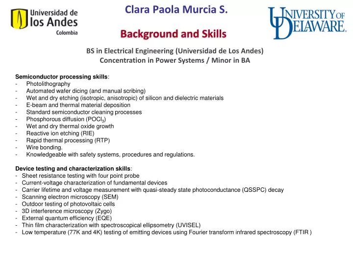
Clara Paola Murcia S. Background and Skills. BS in Electrical Engineering (Universidad de Los Andes) Concentration in Power Systems / Minor in BA Semiconductor processing skills : Photolithography Automated wafer dicing (and manual scribing )

E N D
Clara Paola Murcia S. Background and Skills • BS in Electrical Engineering (Universidad de Los Andes) • Concentration in Power Systems / Minor in BA • Semiconductor processing skills: • Photolithography • Automated wafer dicing (and manual scribing) • Wet and dry etching (isotropic, anisotropic) of silicon and dielectric materials • E-beam and thermal material deposition • Standard semiconductor cleaning processes • Phosphorous diffusion (POCl3) • Wet and dry thermal oxide growth • Reactive ion etching (RIE) • Rapid thermal processing (RTP) • Wire bonding. • Knowledgeable with safety systems, procedures and regulations. • Device testing and characterization skills: • Sheet resistance testing with four point probe • Current-voltage characterization of fundamental devices • Carrier lifetime and voltage measurement with quasi-steady state photoconductance (QSSPC) decay • Scanning electron microscopy (SEM) • Outdoor testing of photovoltaic cells • 3D interference microscopy (Zygo) • External quantum efficiency (EQE) • Thin film characterization with spectroscopical ellipsometry (UVISEL) • Low temperature (77K and 4K) testing of emitting devices using Fourier transform infrared spectroscopy (FTIR )
THz emission from p-doped Si (MS) Motivation New sources and materials need to be developed and characterized in the “terahertz gap” 3 to 30 Lack of emitters in the THz regime. Previous results reported edge emission. Top emitters are easily integrated to other optoelectronic devices
Thin silicon solar cells can be higher efficiency than thick silicon with the same materials properties due to reduced bulk recombination that leads to higher voltages Thin Silicon Solar Cells Planar Thin Silicon Solar Cells • A high performance thin silicon solar cell is based on a high open circuit voltage design . • The light trapping consists of a back surface and reflector that can be independently optimized and a front surface texture and ARC • The thin Si solar cell is grown on high quality material then transferred to a holding substrate. Ideal Thin Si Solar Cell X SEM of 18um thin Si solar cell Light Trapping Passivation High Performance Thin Si Solar Cells (PhD) Solar Cell Thin Silicon Solar Cell Results • IQE is applied to measure critical thin Si solar cell parameters • Design rules for high performance developed and demonstrated • Best Parameters (18um solar cell): • Voc: 631mV • Jsc (1 pass): 22mA/cm2 • FF:81.7% Contact -Reflector PhD Students C. Paola Murcia and Ruiying Hao. Epitaxial layers grown by collaborative research with AmberWave Inc. QE before ARC