Download
1 / 53
550 likes | 728 Vues
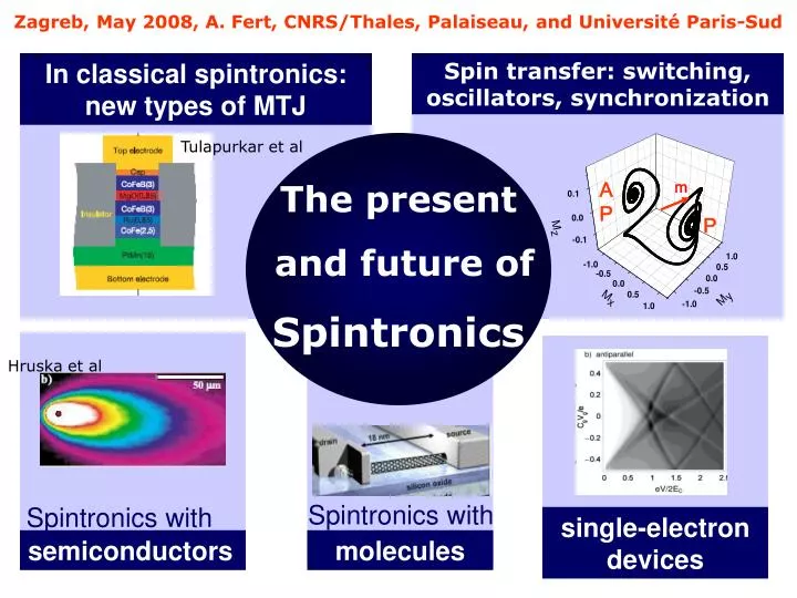
Spin transfer: switching, oscillators, synchronization. AP. m. P. Spintronics with. Spintronics with. single-electron devices. semiconductors. molecules. Zagreb, May 2008, A. Fert, CNRS/Thales, Palaiseau, and Université Paris-Sud. In classical spintronics: new types of MTJ.

E N D
Spin transfer: switching, oscillators, synchronization AP m P Spintronics with Spintronics with single-electron devices semiconductors molecules Zagreb, May 2008, A. Fert, CNRS/Thales, Palaiseau, and Université Paris-Sud In classical spintronics: new types of MTJ Tulapurkar et al The present and future of Spintronics Hruska et al
Introduction : Spin dependent conduction in ferromagnetic conductors, Giant Magnetoresistance (GMR), Tunnel Magnetoresistance (TMR)
Spin dependent conduction in ferromagnetic metals (two current model) Mott, Proc.Roy.Soc A153, 1936 Fert et al, PRL 21, 1190, 1968 Loegel-Gautier, JPCS 32, 1971 Fert et al,J.Phys.F6, 849, 1976 Dorlejin et al, ibid F7, 23, 1977 n (E) EF E I = / or = ( - )/ ( + ) = ( - 1)/( + 1) n (E) I 0.3 n (E) Cr d level = / EF Ni d band Virtual bound state 20 E Ni d band n (E) Cr d level Ti V Cr Mn Fe Co Ni
Mixing impurities A and B with opposite or similar spin asymmetries: the pre-concept of GMR Example: Ni + impurities A and B(Fert-Campbell, 1968, 1971) 1st case2d case A > 1, B< 1 A andB> 1 High mobility channel low spin spin spin spin AB >> A+ B AB A+ B J. de Physique 32, 1971 =/
Magnetic multilayers Fe Cr Fe Cr Fe
Magnetic multilayers Magnetizations of Fe layers at zero field in Fe/Cr multilayers Fe Cr Fe Cr Fe P. Grünberg, 1986 antiferromagnetic interlayer coupling
Magnetic multilayers Magnetizations of Fe layers in an applied field in Fe/Cr multilayers H Fe Cr Fe Cr Fe P. Grünberg, 1986 antiferromagnetic interlayer coupling
Giant Magnetoresistance (GMR) (Orsay, 1988, Fe/Cr multilayers, Jülich, 1989, Fe/Cr/Fe trilayers) Jülich Orsay Resistance ratio ~ + 80% V=RI Magnetic field (kGauss) Current AP (AntiParallel) P(Parallel)
Giant Magnetoresistance (GMR) (Orsay, 1988, Fe/Cr multilayers, Jülich, 1989, Fe/Cr/Fe trilayers) Anti-parallel magnetizations (zero field, high resistance) Resistance ratio Fe Cr Fe ~ + 80% Parallel magnetizations (appl. field, low resist.) net current Magnetic field (kGauss) Fe Cr Fe Condition for GMR: layer thickness nm Current AP (AntiParallel) P(Parallel)
Read head of hard disc drive voltage current Recent review : « The emergence of spintronics in data storage » Chappert, AF et al Nat. Mat.(Nov.07) Magnetic fields generated by the media track 0 5 nm GMR sensor 1997 (before GMR) : 1 Gbit/in2 , 2007 : GMR heads ~ 600 Gbit/in2
Magnetic Tunnel Junctions,Tunneling Magnetoresistance (TMR) 0.1 m tunneling barrier (insulator) ~ 100 nm ferromagnetic electrodes AP P Jullière, 1975, low T, hardly reproducible Low resistance state High resistance state Moodera et al, 1995, Miyasaki et al,1995, CoFe/Al2O3/Co, MR 30-40% Applications: - read heads of Hard Disc Drive - M-RAM (Magnetic Random Access Memory) : density/speed of DRAM/SRAM + nonvolatilty + low energy consumption MRAM
Epitaxial magnetic tunnel junctions (MgO, etc) First examples on Fe/MgO/Fe(001): CNRS/Thales (Bowen, AF et al, APL2001) Nancy (Faure-Vincent et al, APL 2003) Tsukuba (Yuasa et al, Nature Mat. 2005) IBM (Parkin et al, Nature Mat. 2005) ….etc Yuasa et al, Fe/MgO/Fe Nature Mat. 2005 ΔR/R = (RAP-RP)/ RP 200% at RT Clearer picture of the physics of TMR: what is inside the word « spin polarization »? CoFeB/MgO/CoFeB, ΔR/R 500% at RT in several laboratories in 2006-2007 2006-2007 +
Mathon and Umerski, PR B 1999 Mavropoulos et al, PRL 2000 Butler et al , PR B 2001 Zhang and Butler, PR B 2004 [bcc Co/MgO/bcc Co(001)] 1 P 2’ 5 AP 1 2’ 5
Zhang and Butler, PR B 2004 Beyond MgO • MgO, ZnSe (Mavropoulos et al, PRL 2000), etc • 1symmetry (sp) slowly decaying • tunneling of Co majority spin electrons SrTiO3 and other d-bonded insulators (Velev et al , PRL 95, 2005; Bowen et al, PR B 2006) • 5symmetry (d) slowly decaying • tunneling of Co minority spin electrons in agreement with the negative polarization of Co found in TMR with SrTiO3 ,TiO2and Ce1-xLaxO2 barriers(de Teresa, A.F. et al, Science 1999) 1 P 2’ 5 AP 1 2’ 5
Zhang and Butler, PR B 2004 Beyond MgO • MgO, ZnSe (Mavropoulos et al, PRL 2000), etc • 1symmetry (sp) slowly decaying • tunneling of Co majority spin electrons SrTiO3 and other d-bonded insulators (Velev et al , PRL 95, 2005; Bowen et al, PR B 2006) • 5symmetry (d) slowly decaying • tunneling of Co minority spin electrons in agreement with the negative polarization of Co found in TMR with SrTiO3 ,TiO2and Ce1-xLaxO2 barriers(de Teresa, A.F. et al, Science 1999) 1 P 2’ 5 AP 1 2’ 5 Physical basis of « spin polarization »(SP) ¤Tunneling:SP of the DOS for the symmetry selected by the barrier ¤Electrical conduction: SP depends on scatterers, impurities,..
Spin Transfer (magnetic switching, microwave generation) Spintronics with semiconductors Spintronics with molecules
Spin Transfer (magnetic switching, microwave generation) Spintronics with semiconductors Spintronics with molecules Common physics: spin accumulation spins injected to long distances by diffusion
Co/Cu: Current to Plane (CPP) -GMRof multilayered nanowires(L.Piraux, AF et al, APL 1994,JMMM 1999) CPP-GMR subsists at almost 1m 100 nm MR ratio (%) 10 8 6 Co thickness (nm) 4 CPP-GMR scaling length = spin diffusion length >> mean free path spin accumulation theory (Valet-Fert, PR B 1993) 2 CIP-GMR scaling length = mean free path 0 200 0 100 300 400 500 400 nm Other results: MSU group, PRL 1991, JMMM 1999
Spin injection/extraction at a NM/FM interface (beyond ballistic range) NM (illustration in the simplest case = flat band, low current, no interface resistance, single polarity) FM zone of spin accumulation = spin diffusion length in FM = spin diffusion length in NM (example: 0.5 m in Cu, >10m in carbon nanotube) E EF = spin chemical potential Spin accumulation = EF-EF EF-EF~ exp(z/ ) in FM z EF-EF~ exp(-z/ ) in NM EF EF= spin chemical potential Spin current = J-J J-J = current spin polarization J+J z
Spin injection/extraction at a NM/FM interface (beyond ballistic range) NM (illustration in the simplest case = flat band, low current, no interface resistance, single polarity) FM zone of spin accumulation = spin diffusion length in FM = spin diffusion length in NM (example: 0.5 m in Cu, >10m in carbon nanotube) E EF Spin accumulation = EF-EF • Extension to more complex situations • -CPP-GMR: typical multi-interface problem (spin accumulation overlaps) • Spin transfer: multi-interface problem with non-colinear magnetic configurations • Spintronicswith semiconductors: spin inject. from metals complicated by « density of states mismatch », band bending, etc z EF EF Spin current = J-J J-J J+J z
Spin injection/extraction at a Semiconductor/FM interface 1) situation without interface resistance (« conductivity mismatch ») (Schmidt et al, PR B 2000) NM = metal or semiconductor FM zone of spin accumulation E Semiconductor/ F metal If similar spin spliting on both sides but much larger density of states in F metal much larger spin accumulation density and much more spin flips on magnetic metal side almost complete depolarization of the current before it enters the SC EF Spin accumulation = EF-EF z EF EF Spin current = J-J NM= metal NM = semiconductor z
Spin injection/extraction at a Semiconductor/FM interface spin dependent. interf. resist. (ex:tunnel barrier) NM = semiconductor FM e- Spin dependent drop of the electro-chemical potential Discontinuity increases the spin accumulation in NM z EF EF re-balanced spin relaxations in F and NM EF EF Spin accumulation = EF-EF Current Spin Polarization (J-J)/(J+J) extension of the spin-polarized current into the semiconductor Rasbah, PR B 2000 A.F-Jaffrès, PR B 2001
Spin transfer (J. Slonczewski, JMMM 1996, L. Berger, PR B 1996) Ex:Cobalt/Copper/Cobalt S
Spin transfer (J. Slonczewski, JMMM 1996, L. Berger, PR B 1996) Ex:Cobalt/Copper/Cobalt S The transverse component of the spin current is absorbed and transferred to the total spin of the layer j M x (M x M0) Torque on S Mx(MxM0) S
Experiments on pillars Au Free ferro 4 nm Cu 10 nm • First regime (low H): irreversible switching (CIMS) • Second regime (high H): steady precession(microwave generation) Fixed ferro I - Cu V - Metallic pillar 50x150 nm² Au Free ferro 4 nm barrier 10 nm Fixed ferro I - Cu V - Tunnel junction E-beam lithography + etching
Regime of irreversible magnetic switching AP state of m First experiments on pillars: Cornell (Katine et al, PRL 2000) CNRS/Thales (Grollier et al, APL 2001) IBM (Sun et al, APL 2002) M m AP P P state of m GaMnAs/InGaAs/GaMnAs tunnel junction(MR=150%) Py/Cu/Py 50nmX150nm (Boulle, AF et al) (Elsen, AF et al, PR B 2006) H=7 Oe RT 30 K AP P typical switching current 107A/cm2 switching time can be as short as 0.1 ns (Chappert et al) 1 x 10⁵ A/cm2 Py = permalloy
Regime of steady precession (microwave frequency range) CNRS/Thales, Py/Cu/PY (Grollier et al) (Py = permalloy) AP H Hd M Hd P m b Hd Increasing current
Regime of steady precession or vortex motion(microwave frequency range) CoFeB/MgO/CoFeB junction(J.Grollier, AF et al 2008, collaboration S. Yuasa et al, AIST) 90 H = -303G 1.40mA PSDmax = 50 nW/GHz width=8MHZ Lorentzian fit 60 PSDmax = 90 nW/GHz width=62MHZ PSD (nW/GHz) 30 0 H 4.5 5.0 5.5 AP Frequency (GHz) ~ 20 – 30 nm Frequency (MHz) M P m PSD (nW/mA2GHz) Low frequency vortex excitation in Py/Au/Co nanocontacts(M.Darques, AF et al, 2008) MgO
Regime of steady precession or vortex motion(microwave frequency range) CoFeB/MgO/CoFeB junction(J.Grollier, AF et al 2008, collaboration S. Yuasa et al, AIST) Spin Transfer mixes very different (and interacting) problems: transport (in metallic pillars, tunnel junctions, point contacts) problems of non-linear dynamics micromagnetism (non-uniform excitations, vortex motion..) 90 H = -303G 1.40mA Lorentzian fit 60 PSDmax = 90 nW/GHz width=62MHZ PSD (nW/GHz) 30 0 4.5 5.0 5.5 Frequency (GHz) PSDmax = 50 nW/GHz width=8MHZ PSD (nW/mA2GHz) Low frequency vortex excitation in Py/Au/Co nanocontacts(M.Darques, AF et al, 2008) Frequency (MHz)
Co/Cu/Py (« wavy » angular variation calculated byBarnas, AF et al, PR B 2005) Py/Cu/Py (standard) Au Py (8nm, free) Cu ( 8nm) 100x170nm² Co (8nm, fixed) IrMn (15nm) or CoO or Cu free Py:fast spin relaxation fixedCo: slower spin relaxation Negative I (mA) H 0 H 0 (2 Oe) Boulle, AF et al, Nature Phys. 2007 oscillations at H=0 Positive I
Switching of reprogrammable devices (example: MRAM) 1) By external magnetic field (present generation of MRAM, nonlocal, risk of « cross-talk » limits integration) Current pulse 2) «Electronic» reversal by spin transfer from current (ST-MRAM: next generation of MRAM, with demonstrations by Sony, Hitachi, NEC, etc)
Spin Transfer Oscillators (STO) (communications, microwave pilot) • Advantages: • direct oscillation in the microwave range (5-40 GHz) • agility: control of frequency by dc current amplitude, (frequency modulation , fast switching) • high quality factor • small size ( 0.1m) (on-chipintegration) • oscillations without applied field • Needed improvements • - - increase of power by synchronization of a large of number N of STO ( x N2 ) f/ff 18000 Rippart et al, PR B70, 100406, 2004
Experiments of STO synchronization by electrical connection (B.Georges, AF et al, CNRS/Thales and LPN-CNRS, preliminary results) Ihf1+ Ihf2 increasing I trilayer 2 + + Idc Ihf1 Ihf2 trilayer 1 hf circuit Idc
Spintronics with semiconductors and molecules
Spintronics with semiconductors Magnetic metal/semiconductor hybrid structures Example: spin injection from Fe into LED (Mostnyi et al, PR. B 68, 2003) Ferromagnetic semiconductors (FS) GaMnAs (Tc170K) and R.T. FS Electrical control of ferromagnetism TMR, TAMR, spin transfer (GaMnAs) Field-induced metal/insulator transition
Spintronics with semiconductors Magnetic metal/semiconductor hybrid structures Spin Field Effect Transistor ? Ferromagnetic semiconductors (FS) Example: spin injection from Fe into LED (Mostnyi et al, PR. B 68, 2003) V F2 F1 Semiconductor channel Semiconductor lateral channel between spin-polarized source and drain transforming spin information into large(?) and tunable (by gate voltage) electrical signal GaMnAs (Tc170K) and R.T. FS Electrical control of ferromagnetism TMR, TAMR, spin transfer (GaMnAs) Field-induced metal/insulator transition
P F2 F1 AP Semiconductor channel Nonmagnetic lateral channel between spin-polarized source and drain Semiconductor channel: « Measured effects of the order of 0.1-1% have been reported for the change in voltage or resistance (between P and AP)…. », from the review article « Electrical Spin Injection and Transport in Semiconductors » by BT Jonker and ME Flattéin Nanomagnetism (ed.: DL Mills and JAC Bland, Elsevier 2006)
Nonmagnetic lateral channel between spin-polarized source and drain Semiconductor channel: « Measured effects of the order of 0.1-1% have been reported for the change in voltage or resistance (between P and AP)…. », from the review article « Electrical Spin Injection and Transport in Semiconductors » by BT Jonker and ME Flattéin Nanomagnetism (ed.: DL Mills and JAC Bland, Elsevier 2006) Carbon nanotubes: R/R 60-70%, VAP-VP 20-60 mV LSMO LSMO L.Hueso, N.D. Mathur,A.F. et al, Nature 445, 410, 2007 P F2 F1 MR 72% AP Semiconductor channel nanotube 1.5 m LSMO = La2/3Sr1/3O3
Nonmagnetic lateral channel between spin-polarized source and drain Semiconductor channel: « Measured effects of the order of 0.1-1% have been reported for the change in voltage or resistance (between P and AP)…. », from the review article « Electrical Spin Injection and Transport in Semiconductors » by BT Jonker and ME Flattéin Nanomagnetism (ed.: DL Mills and JAC Bland, Elsevier 2006) Carbon nanotubes: R/R 60-70%, VAP-VP 20-60 mV LSMO LSMO L.Hueso, N.D. Mathur,A.F. et al, Nature 445, 410, 2007 AP 60% P F2 F1 AP Semiconductor channel nanotube 1.5 m P P LSMO = La2/3Sr1/3O3
Two interface spin transport problem (diffusive regime) Condition dwell time n < spin lifetime sf Condition dwell time n < spin lifetime sf Condition for spin injection Condition for spin injection AF and Jaffrès PR B 2001* +cond-mat 0612495, + IEEE Tr.El.Dev*. 54,5,921,2007 *calculation. for Co and GaAs at RT 1.6 1.2 0.8 0.4 0.0 1.6 1.2 0.8 0.4 0.0 R/RP R/RP L L L=20nm L=20nm L L Interface resistance rb* in most experiments V V F2 F2 F1 F1 Semiconductor channel Semiconductor channel L L Window only for lsf(N) > L
Nanotubes (also graphene, other molecules) : Semiconductors:
Nanotubes (also graphene, other molecules) : Semiconductors: Solution for semiconductors: shorter L ?, larger transmission tr ?
Nanotubes (also graphene, other molecules) : Semiconductors: Potential of molecular spintronics (nanotubes, graphene and others) Solution for semiconductors: shorter L ?, larger transmission tr ?
Nanotubes (also graphene, other molecules) : Semiconductors: Potential of molecular spintronics (nanotubes, graphene and others) Solution for semiconductors: shorter L ?, larger transmission tr ? Next challenge for molecules: spin control by gate
Summary ¤Already important aplications of GMR/TMR (HDD, MRAM..)and now promising new fields SILICON ELECTRONICS • Spin transfer formagnetic switching and microwave generation • Spintronics with semiconductors, molecules or nanoparticles SPINTRONICS
Acknowledgements to M. Anane, C. Barraud, A. Barthélémy, H. Bea, A. Bernand-Mantel, M. Bibes,O. Boulle, K.Bouzehouane, O. Copi, V.Cros, C. Deranlot, B. Georges, J-M. George, J.Grollier, H. Jaffrès, S. Laribi, J-L. Maurice, R. Mattana, F. Petroff, P. Seneor, M. Tran F. Van Dau, A. Vaurès Université Paris-Sud and Unité Mixte de Physique CNRS-Thales, Orsay, France P.M. Levy, New York Un., A.Hamzic, M. Basletic Zagreb University B. Lépine, A. Guivarch and G. Jezequel Unité PALMS, Université de Rennes , Rennes, France G. Faini, R. Giraud, A. Lemaître: CNRS-LPN, Marcoussis, France L. Hueso, N.Mathur, Cambridge J. Barnas,M. Gimtra, I. Weymann, Poznan University
Two interface spin transport problem (diffusive regime) Condition dwell time n < spin lifetime sf Condition dwell time n < spin lifetime sf Condition for spin injection Condition for spin injection AF and Jaffrès PR B 2001* +cond-mat 0612495, + IEEE Tr.El.Dev*. 54,5,921,2007 *calculation. for Co and GaAs at RT 1.6 1.2 0.8 0.4 0.0 1.6 1.2 0.8 0.4 0.0 R/RP R/RP L L L=20nm L=20nm L L V V GaMnAs/AlAs/GaAs/AlAs/GaMnAs vertical structure F2 F2 F1 F1 Semiconductor channel Semiconductor channel L L Window only for lsf(N) > L
VG VSD eV = 25-500 meV >> Coulomb energy, level spacing, spin-orbit spliting, 4.2 K< T <120 K E+Uc source source drain drain nanotube nanotube LSMO/CNT/LSMO: higher voltage experiments thanks to large interface resistances and small V2/R heating at large V Usual conditions: small bias voltage experiments Uc=e2/2C eV 1 meV Oscillatory variation of the conductance, different signs of theMR depending on the bias voltage and from sample to sample Quasi-continuous DOS, same conditions as for semiconductor or metallic channel
Deviations from at large current density (drift effect) = low current limit = deviations from the low current limit (nondegenerate semiconductor) J-J J+J current density from Jaffrès and A.F. (see also Yu and Flatté)
Condition dwell time n < spin lifetime sf Condition for spin injection r r R R II 1.6 1.2 0.8 0.4 0.0 R/RP L R (), r ()=interface resistance (equal for source and drain) L=20nm I III L II III I r r P P V/2 Unpolarized current in the semiconductor (depolarization in the source and repolarization in the drain) V/2 R R r R r R AP r r R R R/R = 0 Optimal R/R R/R = 0