Download
1 / 24
250 likes | 409 Vues
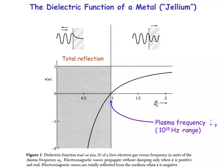
Total reflection. The Dielectric Function of a Metal (“Jellium”). Plasma frequency p ( 10 15 Hz range). E p. Why are Metals Shiny ?.

E N D
Total reflection The Dielectric Function of a Metal (“Jellium”) Plasma frequency p (1015Hz range)
Ep Why are Metals Shiny? An electric field cannot exist inside a metal, because metal electrons follow the field until they have compensated it. An example is the image charge, which exactly cancels the field of any external charge. This is also true for an electromagnetic wave, where electrons respond to the changing external field. As a result, the electromagnetic wave cannot enter a metal and gets totally reflected in the region with <0. Above the plasma frequency, however, the external field oscillates too fast for the electrons to follow. A metal loses its reflectivity. The corresponding photon energy is the plasmon energy Ep = ħp, typically 10-30 eV (deep into the ultraviolet). The reflectivity of aluminum cuts off at its plasmon energy Data (dashed) are compared to the jellium model (full). The difference is due to damping of the electrons in real metals.
Plasma Frequency and Energy-Saving Window Coatings The reflectivity cutoff at the plasmon energy can be used for energy-saving window coatings which transmit visible sunlight (photon energy above Ep), but reflect thermal IR radiation back into a heated room. To get a reflectivity cutoff in the infraredone needs a smaller electron density than in a metal. A highly-doped semiconductor fits just right, such as indium-tin-oxide (ITO). This material is also widely used as transparent front electrode for solar cells, LEDs, and liquid crystal displays. An ITO film transmits visible light and reflects thermal infrared radiation, keeping the heat inside a building. R = Reflectivity T = Transmission Compared to the previous slide the the x-scale is inverted ( instead of E, with 1/E)
What is a Plasmon? A plasmon is a density wave in an electron gas. It is analogous to a sound wave, which is a density wave in a gas consisting of molecules. Plasmons exist mainly in metals, where electrons are weakly bound and free to roam. The free electron gas (jellium) model provides a good approximation. The electrons in a metal can wobble like a piece of jelly, pulled back by the attraction of the positive metal ions that they leave behind. In contrast to the single electron wave function that we encountered already, a plasmon is a collective wave. Billions of electrons oscillate in sync.
The electron gas has a resonance right at the plasma frequency p . This resonance frequency increases with the electron density n, since the electric restoring force is proportional to the displaced charge (analogous to the force constant f of a spring): p n Surface Plasmon Bulk Plasmon k k The Plasmon Resonance
1 E 2 E-E 3 e- 4 5 bulk surface E = Observation of Plasmons Plasmons can be observed by electron energy loss spectroscopy (EELS). Electrons with an energy of several keV are reflected from a metal surface and lose energy by exciting 1, 2, 3, … plasmons. Large peaks at multiples of 15.3eV are from bulk plasmons, and the smaller peaks at multiples of 10.3eV from surface plasmons. The surface plasmon energy is 2 times lower than the bulk plasmon energy.
Photon Bulk Plasmon Surface Plasmon Static: 0 0 Quantum Numbers of Plasmons Like any other particle/wave in a solid,aplasmon has energy E=ħ and momentum p=ħkas quantum numbers. The same E(k) plots can be used as for individual electrons and phonons. The surface plasmon band joins the photon band at very small k and . The limit 0describes the image charge.
Coupling of Light and Plasmons To combine optoelectronics with plasmonics one has to convert light (photons) into plasmons. This is not as simple as it sounds. Bulk plasmons are longitudinal oscillations (parallel to the propa-gation direction), while photons are transverse (perpendicular to the propagation). They don’t match. Surface plasmonsare transverse, but they are mismatched to photons in their momentum. The two E(k) curves only coincide at k=0. It is possible to provide the necessary momentum ħk by a grating, which transfers the k=2/d (d=line spacing). Thereby one can control the wavelength of surface plasmons.
Gold film Attenuated Total Reflection Another method to couple photons and surface plasmons uses attenuated total reflection at a metal-coated glass surface. The exponentially damped (evanescent) light wave escaping from the glass can be matched to a surface plasmon (or thin film plasmon) in the metal coating. This technique is surface sensitive and is used for bio-sensors.
Low-Dimensional Plasmons in Nanostructures The same way as the energy of single electron waves becomes quantized byconfinement in a nanostructure, plasmons are affected by the boundary conditions in a thin film or a nano-particle. Plasmons in metal nanoparticles are often called Mie-resonances, after Gustav Mie who calculated them hundred years ago. Their resonance energy and color depend strongly on their size, similar to the color change induced in semiconductor nanoparticles by confinement of single electrons. In both cases, smaller particles have higher resonance energy (blue shift).
Nanotechnology in Roman Times: The Lycurgus Cup Plasmons of gold nanoparticles in glass reflect green, transmit red.
Plasmonics • Optoelectronics is much faster than regular electronics • (waveguides, optical fibers). • But the long wavelength of light (≈m) creates a problem • for extending optoelectronicsinto the nanometer regime. • A possible way out is the conversion of light into plasmons. • They have much shorter wavelengththan light (larger k).
Plasmonic Waveguide (“Wire”) Consisting of a String of Gold Nanoparticles Calculated electric field of an electromagnetic pulse propagating along a string of gold nanoparticles The energy is transferred between neighboring gold particles by coupled Mie-resonances.
Polariton band gap Polariton = Photon + Phonon A polariton is an phonon that interacts with photons. Its E(k) plot shows an avoided crossing between the pure photon band (dashed) and the pure TO phonon band (similar to the surface plasmon). An avoided crossing is always a sign that two bands interact. At the crossing, a bonding and an antibonding combination of the bands is formed. Their splitting is comparable to the interaction energy. Since a photon is always transverse, it interacts with the transverse optical (TO) phonon, not with the longitudinal optical (LO) phonon. Indeed, the crossing with the LO band is not avoided.
Total reflection The photon resonates with the transverse optical phonon fre-quency T (both transverse). This plot becomes similar to that for a plasmon (next slide) if one shifts the resonance to T = 0. L is equivalent to p . Indeed, both waves are longitudinal. polariton band gap Longitudinal phonon frequency Transverse phonon frequency This plot looks similar to the previous plot,but it is 900 rotated: () vs.(k) Polaritons and the Dielectric Function
Total reflection Plasma frequency (longitudinal) Resonance at =0 (transverse) A look back at the Dielectric Function of a Metal
0 p s Resonances in the Dielectric Constant The dielectric constant is a complex number: =1+i2 The real part 1describes refraction of light (an elastic process) The imaginary part2describes absorption(inelastic, E 0). A bulk plasmon occurs at p=L where 1=0. A surface plasmon occurs at s where 1=-1. (More precisely: Im[1/] and Im[1/(+1)]have maxima.) General behavior of the dielectric constant () for a damped oscillator with resonance frequency 0, static dielectric constant st , asymptotic di-electric constant(n2, n=refractive index in the visible), and damping constant >0: ()= + 02(st-)/(02-2-i)
The Dielectric Constant over a Wide Frequency Range Static Dipoles Phonons Electrons (optical) (in atoms) Static Microwaves Infrared Ultraviolet
Photonics In photonics one tries to manipulate the dielectric constant by creating artificial resonators via nano-structured dielectric materials (“metamaterials”). Just above the resonance there is a region with <0 where light is totally reflected (Slide 15). This total reflection region can be viewed as a band gap in the E(k) relation of polaritons (Slide 14), analogous to the band gap of electrons in a semiconductor. An artificial crystal lattice made from polystyrene beads (similar to an opal, an iridescent gemstone). The photonic band gap causes a reflectance maximum.
Cloaking: Making an Object Invisible Surrounding an object with a material having the right kind of dielectric properties (negative refractive index) can make the object invisible. A B Cloaking simulation in two dimensions: A. The black disc blocks the light coming from the left and reflects it back, leaving a shadow towards the right (shown in light green + yellow). B. The surrounding ring of cloaking material guides the light around the disc. Reflection and shadow are avoided,thereby avoiding any trace of the object.
Cloaking: Are Harry Potter’s Tricks Possible? • There is still some debate how far one can push the idea of cloaking by materials with a negative refractive index. • Some observations: • Cloaking works perfectly only at one wavelength, due to the need for a sharp resonance to create negative n. • So far, it works mainly with microwaves, because the resonators required for visible light would have to be well below a micrometer in size. • When cloaking just the intensity (but not phase and polarization), the task becomes much simpler. • If nobody can look through the cloak, can the person wearing it look out?
1 m Actual Metamaterials Most metamaterials with negative refractive index have been made for microwaves (below left). Such devices are interesting for making an airplane invisible to radar(wavelength 3cm). To produce analogous metamaterials for visible light requires nanotechnology with structures small compared the wavelength of light (above right). Even with that under control, it is hard to cloak an object at all wavelengths. Metamaterials are active only near a resonance, which occurs at a particular wavelength.
The Perfect Lens A medium with refractive index n=-1 acts as perfect lens. For n== -1 both and need to be negative. =- Lens Negative nrefracts light towards the same side of the normal (not the opposite side).