Download
1 / 3
30 likes | 198 Vues
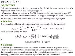
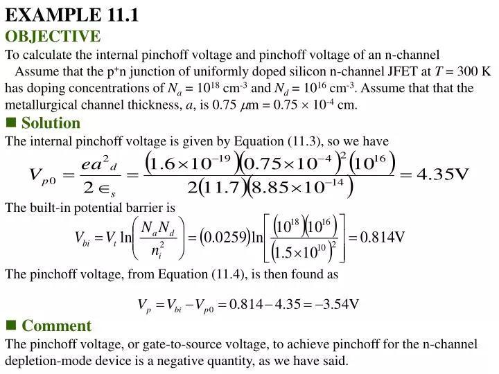
EXAMPLE 11.1 OBJECTIVE To calculate the internal pinchoff voltage and pinchoff voltage of an n-channel

E N D
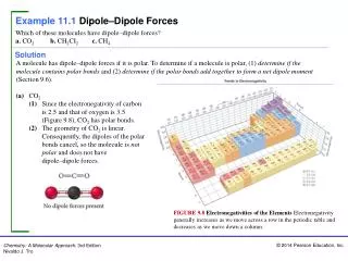
EXAMPLE 11.1 • OBJECTIVE • To calculate the internal pinchoff voltage and pinchoff voltage of an n-channel • Assume that the p+n junction of uniformly doped silicon n-channel JFET at T = 300 K has doping concentrations of Na = 1018 cm-3 and Nd = 1016 cm-3. Assume that that the metallurgical channel thickness, a, is 0.75 m = 0.75 10-4 cm. • Solution The internal pinchoff voltage is given by Equation (11.3), so we have The built-in potential barrier is The pinchoff voltage, from Equation (11.4), is then found as • Comment The pinchoff voltage, or gate-to-source voltage, to achieve pinchoff for the n-channel depletion-mode device is a negative quantity, as we have said.
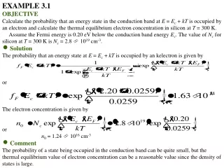
EXAMPLE 11.2 • OBJECTIVE • Design the channel doping concentration and metallurgical channel thickness to achieve a given pinchoff voltage. • Consider a silicon p-channel pn JFET at T = 300 K. Assume that the gate doping concentration is Nd = 1018 cm-3. Determine the channel doping concentration and channel thickness so that the pinchoff voltage is Vp = 2.25 V. • Solution There is not a unique solution to this design problem. We will pick a channel doping concentration of Na = 2 1016 cm-3 and determine the channel thickness. The built-in potential barrier is From Equation (11.8), the internal pinchoff voltage must be Vp0 = Vbi + Vp = 0.832 + 2.25 = 3.08 V and from Equation (11.6), the channel thickness can be determined as • Comment • If the channel doping concentration chosen where larger, the required channel thickness would decrease; a very small value of channel thickness would be difficult to fabricate within reasonable tolerance limits.
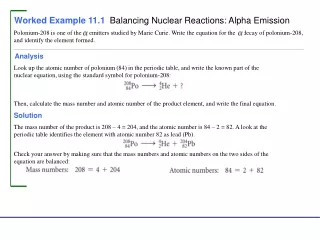
EXAMPLE 11.3 • OBJECTIVE • To calculate the cutoff frequency of a GaAs JFET. Consider a GaAs JFET with the following parameters: n = 8000 cm2/V-s, Nd = 1016 cm-3, a = 0.50 m, and L = 2 m. • Solution Substituting the parameters in Equation (11.18), we have or fT = 110 GHz • Comment • This example shows that GaAs JFETs can have large cutoff frequencies.