Download
1 / 28
280 likes | 450 Vues
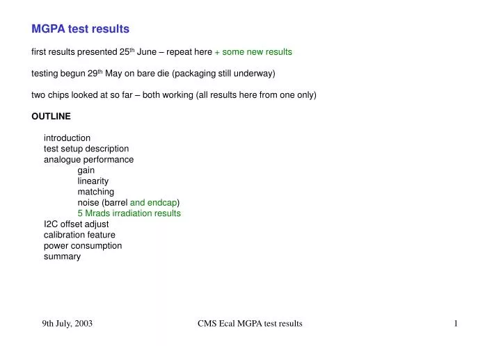
MGPA test results first results presented 25 th June – repeat here + some new results testing begun 29 th May on bare die (packaging still underway) two chips looked at so far – both working (all results here from one only) OUTLINE introduction test setup description

E N D
MGPA test results first results presented 25th June – repeat here +some new results testing begun 29th May on bare die (packaging still underway) two chips looked at so far – both working (all results here from one only) OUTLINE introduction test setup description analogue performance gain linearity matching noise (barrel and endcap) 5 Mrads irradiation results I2C offset adjust calibration feature power consumption summary CMS Ecal MGPA test results
MGPA target specifications simulation results OK for mid and high gain ranges (low gain not a problem) technology spec. for resistors used OK OK CMS Ecal MGPA test results
transconductance gain stages MGPA main features 3 gain channels 1:6:12 differential outputs -> multi-chan. ADC pulse shaping (external components) RfCf = 2RICI = 40 nsec. choose RfCf for barrel/endcap calibration facility prog. amplitude (simple DAC) needs external trigger I2C interface to programme: output pedestal levels enable calibration feature cal DAC setting diff. O/P stages I2C and offset generator RI CI VCM RG1 RI DAC RI CI VCM RG2 RI ext. trig. CCAL charge amp. RI CI VCM RG3 I/P RI Rf Cf CMS Ecal MGPA test results
MGPA photo offset gen. die size ~ 4mm x 4mm for packaging in 100 pin TQFP I2C diff. O/P stage hi VI stage mid charge amp lo CMS Ecal MGPA test results
RAL test board packaged chips not yet available but RAL board can take bare die dual purpose design 1) standalone–used here 2) interface to standard DAQ system bias components fixed – no adjustment possible (without changing 0402 components) most results here for barrel feedback components to first stage (except where indicated) CMS Ecal MGPA test results
Test setup for pulse shape measurements diff. probe or single- ended buffered signal note: very fast risetime charge injection -> pulse shape distortion on rising edge due to slew rate limitation at O/P of first stage current source magnitude OK for 10 nsec exponential edge Scope averaging -> 16 bit resolution. Multiple waveforms captured with different DC offsets to remove scope INL effects. O/P I/P first stage amplifier CMS Ecal MGPA test results
Pulse shapes – low gain channel signals up to 60 pC (feedback components for barrel application: 1.2k//33pF) steps not equally spaced (log attenuator) 2 active probes on +ve and –ve outputs (before any buffering) linear range +/- 0.45 V around Vcm (1.25 V nom.) note: Vcm defined by external pot’l divider (5% resistors) so not exactly 1.25 V CMS Ecal MGPA test results
Pulse shapes – all 3 gain ranges CMS Ecal MGPA test results
Differential pulse shape – low gain channel differential probe on chip outputs (before buffering) 60 pC fullscale signal as before differential swing +/- 0.45 V around Vcm corresponds to ~1.8 Volt linear range pedestal subtracted no “obvious” pulse shape distortion due to higher gain channels saturating CMS Ecal MGPA test results
Differential pulse shapes – all 3 gain channels compared – gain ratios 1 : 5.6 : 11.3 (cf 1 : 6 : 12) no obvious interchannel distortion effects CMS Ecal MGPA test results
Linearity and pulse shape matching – high gain channel fullscale signal 5.4 pC pulse shape matching in spec., linearity outside by factor ~2 CMS Ecal MGPA test results
Linearity and pulse shape matching – mid gain channel fullscale signal 10.8 pC smallest signals show slower risetime – needs further investigation CMS Ecal MGPA test results
Linearity and pulse shape matching – low gain channel fullscale signal 61 pC similar (but worse) effect as for mid-gain channel CMS Ecal MGPA test results
Pulse shape matching between gain channels Pulse shape matching definition: Pulse Shape Matching Factor PSMF=V(pk-25ns)/V(pk) Pulse shape matching = [(PSMF-Ave.PSMF)/Ave.PSMF] X 100 Ave.PSMF = average for all signal sizes and gain ranges systematic discrepancies between channels can be due to mismatch in diff. O/P termination components or (more likely here) difference in stray capacitance from PCB layout spec. CMS Ecal MGPA test results
mismatch of stray O/P capacitance likely due to signal routing on test card 1st stage of buffering differential O/P termination components (1% tolerance) CMS Ecal MGPA test results
effect of input capacitance on pulse shape pulse peak shifts by only ~ 3 nsec. => robust to variations in stray capacitance CMS Ecal MGPA test results
Noise measurements use wide bandwidth true rms meter (single ended I/P) => need diff. to singled ended buffer circuitry => extra noise contribution to subtract will also add extra noise filtering endcap results NEW weak dependence on input capacitance as expected estimated errors: ~ 10% high and mid-gain ranges, ~ 20% low gain range (buffer circuitry dominates here) CMS Ecal MGPA test results
Radiation results: pulse shape low mid high pre-rad 5 Mrads 10 keV X-rays (spectrum peak) , dosimetry accurate to ~ 10%, doserate ~ 1 Mrad/hour, no anneal as yet ~ ½ fullscale signal injected for each gain channel ~ 3% reduction in gain after 5 Mrads CMS Ecal MGPA test results
Radiation results: noise no significant change (within errors)after irradiation CMS Ecal MGPA test results
Radiation results: linearity & pulse shape matching high gain channel shown here linearity degraded slightly at extreme edge of range CMS Ecal MGPA test results
I2C pedestal offset adjustment high gain channel shown here (other channels similar) offset setting 0 -> 105 in steps of 5 (decimal) I2C offset setting 0 linear range ~ optimum baseline setting here corresponds to I2C setting ~70 I2C offset setting 105 CMS Ecal MGPA test results
external on-chip Calibration circuit functionality (1) 10k 8 – bit DAC value 0 – 2.5 V 1nF high Rtc 10pF MGPA I/P derived from external pulse mid low distortion on rising edge for low gain channel – somehow related to external 1 nF cap. CMS Ecal MGPA test results
external on-chip Calibration circuit functionality (2) 10k 8 – bit DAC value 0 – 2.5 V with 1 nF without 1 nF 1nF Rtc 10pF MGPA I/P calibration pulse shapes with/without external 1 nF show improvement if removed effect needs further investigation CMS Ecal MGPA test results
main concern so far: high frequency instability (~ 250 MHz) can be introduced on first stage O/P when probing not clear whether problem on chip (no hint during simulation) or could be test board related decoupling components around first stage not as close in as would like VDDP, VS in particular test board for packaged chips should help with diagnosis decoupling closer in (may be cure?) bias currents easy to vary (should give clues) new version of this board also in pipeline will also take test socket CMS Ecal MGPA test results
Power consumption • Current measured in 2.5 V rail supplying test board -> ~ 245 mA • -> chip current + Vcm divider (4mA) + power LED (3mA) • chip current = 238 mA measuring bias currents and multiplying by mirroring ratios -> 235 mA may change if further testing indicates changing bias conditions -> performance improvements worth having CMS Ecal MGPA test results
Summary all results so far for one unpackaged chip, barrel feedback components to first stage gains close to specification (1 : 5.6 : 11.3) pulse shapes good linearity ~ +/- 0.2% (~ 2 x spec.) pulse shape matching within spec. apart from lowest end of mid and low gain ranges no obvious distortion introduced on lower gain channels by higher gain channels saturating => good chip layout noise close to simulation values (< 10,000 (3,500) e for mid and high gain ranges for barrel (endcap)) I2C features (channel offsets, calibration) fully functioning 5 Mrad radiation results – small effects only for more detailed studies need packaged chips CMS Ecal MGPA test results
MGPA – architecture overview V/I gain resistors external components define CR and CSA gain diff. O/P external components define RC offset adjust offset & CAL pulse generation I2C interface CMS Ecal MGPA test results