Download
1 / 67
720 likes | 1.21k Vues
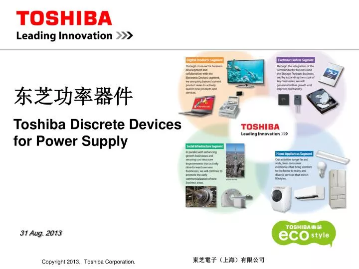
东芝功率器件 Toshiba Discrete Devices for Power Supply. 31 Aug. 2013. 目录. 东芝集团业务简介 东芝分立器件简介 功率器件的发展趋势 (高压 MOS ,低压 MOS ) 新材料功率器件( SiC , GaN ) 电源的拓扑结构 及东芝功率器件的产品线 AC-DC : Flyback , Forward , Half Bridge , Full Bridge

E N D
东芝功率器件 Toshiba Discrete Devices for Power Supply 31 Aug. 2013
目录 • 东芝集团业务简介 • 东芝分立器件简介 • 功率器件的发展趋势(高压MOS,低压MOS) • 新材料功率器件(SiC,GaN) • 电源的拓扑结构及东芝功率器件的产品线 • AC-DC:Flyback,Forward,Half Bridge,Full Bridge • DC-DC:Forward,Push Pull,Half Bridge,Full Bridge(Isolation type) • 东芝官网分立器件参数模拟快速入门 • 销售渠道
通过能源技术和存储技术的创新以及信息技术提供解决方案通过能源技术和存储技术的创新以及信息技术提供解决方案
分立器件简介 C-MOSLogic / 1GateLogic 标准的逻辑器件 Bus Switch Level Shifter MOS FET/BRT Diode(SW/SBD / ESD etc) 小信号分立器件 OP-AMP/Comparator LoadSwIC / Regulator RF Tr / Di SOISwitch 分立器件 Power MOS FET( HV-MOS/LV-MOS) Power MOS FET(HV-MOS / LV-MOS) BJT IGBT / IEGT Power Di(SBD / ZD) 功率器件 Intelligent Power Device(HV-IPD / LV-IPD) CompoundMaterial(SiC / GaNpower) PhotoCoupler FiberCoupler(TOSLINK) 光耦 White LED
大功率器件 工业变频器1700-4500V PMI PPI 牵引、电力转换器、工业变频器 电力机车 变频器 电力转换器
主要的产品 SiC 针对于大功率 1 0.1 HV-MOS Voltage(kV) 重点推出第四代 DTMOSⅣ. LV-MOS GaN U-MOSⅧ 致力于提高效率 高速开关的应用 Frequency(kHz) 1 10 100 1000 10000
东芝功率MOSFET的发展蓝图 VDSS U-MOSⅧ-H(30V) U-MOSⅦ-H(30V) Ⅸ-H U-MOSⅣ U-MOSⅨ-H (40V-120V) 100V U-MOSⅧ-H(60V-120V) U-MOSⅧ-H (150V/200V/250V) 200V p-MOSⅤ p-MOSⅦ (200V / 250V / 300V) 300V p-MOS p-MOSⅦ (400V / 500V / 600V / 650V) DTMOS 400V p-MOSⅥ 500V DTMOSⅤ (500V / 600V / 650V ) DTMOSⅣ HighSpeed Switching DTMOSⅢ(600V) DTMOSⅣ(600V / 650V) Fast Diode added DTMOSⅡ (600V / 650V) 600V DTMOSⅢ(700V/4A) p-MOSⅣ (800V / 900V) HV-DTMOS (800V / 900V ) p-MOSⅧ (800V / 900V) 700V p-MOS 800V 900V 2014 15 CY:2010 2011 2012 2013
东芝功率MOSFET封装发展蓝图 3x3mm for LVMOS(U-MOS series) Both-Side Cooling 5x6mm for LVMOS(U-MOS series) 8x8mm DFN for DTMOS (Since DTMOSⅣ) Standard D-pak since p-MOSⅦ & DT3 Standard I-pak for HVMOS(Since DTMOSⅢ) Standard D2-pak,I2-pak for HVMOS(Since DTMOSⅢ) Standard TO-220 for HVMOS and LVMOS(SR-MOS) TO-220SIS(FP)for HVMOS and LVMOS(SR-MOS) TO-3P(N)for HVMOS(p-MOS / DTMOS) TO-247for DTMOS TO-3P(L)for HVMOS(High Current) CY:2010 2011 2012 2013 2014 15
Super Junction MOSFET(DTMOS)研发趋势 1.Single-EPI(SE)Process Multi EPI Single-EPI DTMOS拥有超低内阻和丰富的封装,可以支持更高效率,更紧凑的电源设计方案 50 A 40 【Ron*A Improvement】 In the same die size RDSon can be reduced“30%” In the same RDSon Die size can reduce 30% B C DTMOSⅠ 30 DTMOSⅡ RonA(mWcm2) DTMOSⅢ B C 20 C Size: ChipSizeRDSon: On resistance New Generations DTMOSⅣ DT4Size=100RDSon=70 10 C Target for future Gen. DTMOSⅤ DT3Size=100RDSon=100 0 DT4Size=70RDSon=100 ‘01 ‘03 ‘05 ‘07 ‘09 ‘11 ‘13 ‘15
DTMOS Ⅳ最新工艺Single-EPI的优势 Single-EPI工艺的优势在于提高了器件的性能 Ron・AImprovement(Normalized) Si limit(88) -MOSⅦ(100%) DTMOSⅢ(ME)(25%) DTMOSⅣ(SE)(16%) ME limit(20) Super Junction Type SE limit(8.8) Single-EPI工艺可使得制程时间减少33% Multi EPI: ▲33% Single-EPI:
DTMOSⅣ性能的优化 New Improvement by Fine patterning and Optimized Vertical profile Optimization Gate layout and structure We will consider the additional line up(other voltage,with HSD etc... )due to the market inquiry
DTMOSⅣ的优势 DTMOSⅣ优化了内阻的温度系数 A1 A2 B1 SE工艺使得在MOS管在较高的结温状态下也能保持较低的内阻,从而可以提高电源模块的效率。 B2
DTMOSⅣ:Eoss Conditions:VDS=0 to 400V,VGS=0,Ta=25℃ DTMOSII:TK20A60U 20%reduction Competitor B Competitor A DTMOSIII:TK18A60V 12%reduction DTMOSIV:TK16A60W Eoss(mJ) 超级结的独特结构造成了较高的输出电容,从而导致电源模块在轻载时效率不好。相比于DTMOSⅢ,DTMOSⅣ的输出电容减少了12%,从而提高了在轻载时的效率。
DTMOSⅣ:效率的评估(120W SMPS) • 相比于其他同规格的竞争者,DTMOSⅣ在所有的功率段都能保持较高的效率 ・Efficiency vs. Output Conditions:120W SPS board PFC stage,Rg=10Ω :DTMOSII 0.19Ωmax :DTMOSIII 0.19Ωmax :DTMOSIV 0.19Ωmax :IPA60R199CP 0.199Ω :IPA60R190C6 0.19Ω :SPA20N60C3 0.19Ω
LVMOS发展蓝图(Silicon) (CY) U-MOSⅦ U-MOSⅧ U-MOSⅨ TPCA8055-H Ron=1.9mOhm(max)@10V TPHR9003NH Ron=0.9mOhm(max)@10V U-MOSⅣ / Ⅵ U-MOSⅨ Ron=0.7m(typ.)@10V in SOP Advance U-MOSⅧ U-MOSⅨ TK100E10N1: Ron=3.4mOhm(max)@10V in TO-220 TPH4R50ANH:Ron=4.5mOhm(max)@10V in SOP Advance Pi-MOSⅤ/ Ⅶ U-MOSⅧ Best-in-class RonCiss U-MOSⅣ U-MOSⅧ RonA=16mΩ*mm2(30V) RonA = 10.8mΩ*mm2 (30V)
U-MOSⅧ-H产品线 U-MOSⅧ-H扩大了产品线,可以满足不同市场的需求
U-MOSⅧ-H效率的对比(LVMOS) TK72E12N1 效率的对比 TK65E10N1 效率的对比 Test condition:120W NBPC ADP,Vin=100VAC,Vout=19.5V Test condition:120W NBPC ADP,Vin= 100VAC, Vout=19.5V VDS=100V VDS=120V TK72E12N1(U-MOSⅧ/120V/4.4mΩ) TK65E10N1(U-MOSⅧ/100V/4.0mΩtyp) Competitor A(120V/4.1mΩ) 优势!! Competitor A(100V/3.9mΩtyp) 优势!! 轻载时TK65E10N1更好! TK72E12N1一直保持了较高的效率!
新材料功率器件 SiC & GaN
复合型原材料的应用领域 1. SiC器件:相比于Si,可以实现低损耗&大容量2. GaN器件:相比于Si,可以实现低损耗&更快的开关速度
Ron・ALimitofSi,SiC,GaN(Theoreticalvalue) Si SiC Ron・A[mΩ・cm2] GaN VDSS[V]
SiC-SBD产品线 *Under development
电源的拓扑结构及 东芝功率器件的产品线
各种应用的开关电源及其电路结构 • 功率MOS管是开关电源的主要的器件 开关电源 AC-DC ResonantHalf/Ful-BridgePower SuppliesUp to around 800W(Constant operating frequency) AC-DC ForwardPower SuppliesUp to around 200W (Constant operating frequency) AC-DC FlybackPower Supplies DC-DC ConvertersIsolatedNon-isolated Output:Around 50W Separately ExcitedUp to around 70W(Constant operating frequency) Self-ExcitedUp to around 40W(Variable operating frequency) • Desktop PCs • Power supplies for • game consoles • Multifunction • printers • Industrial power • supplies • On-board • DC-DC ConvertersNotebook PCs Power supplies for CPUs Regulator circuits Communications equipment • Notebook PC adaptors • Chargers for portable products • LCD adaptors • PC peripherals • Power supplies • Standby power supplies and smalladapters • Power supplies for • FPD TVs • Desktop PCs • Servers
主要的电源拓扑结构 Non-Isolated DC-DC AC-DC(PFC) Secondary side Primary side DC-DC Converter RectifierAC-DC PFC DC-DC Converter ElectricalOutlet DC-DC Converter DC-DCnon-Isolated Flyback Type Forward Type Half-Bridge Type Full-Bridge Type DC-DC Converter
Flyback PFC Output VIN= 220VAC + - + Detect & Compare PFC Control SwitchHigh-voltage MOSFET Control Circuit - Main SwitchHigh-voltage MOSFET Secondary SwitchLow-voltage MOSFET 反击式AC-DC • 反击式AC-DC 反击式的拓扑结构是最简单,且元器件应用最少的一种拓扑,适用于低功率的电源。 AC-DC
+ - + - 正激式AC-DC • 正激式AC-DC Secondary SwitchLow-voltage MOSFET Main SwitchHigh-voltage MOSFET Forward AC-DC PFC Output VIN= 220VAC PFC Control Switch High-voltage MOSFET Detect & Compare Control Circuit
+ - + + + - - - Detect & Compare Control Circuit 半桥式AC-DC • 半桥谐振AC-DC 半桥谐振电源适用于从150W至1kW相对较高的大功率电源应用。两个晶体管与输入供电电压串联连接,降低输入电压适于变压器初级端的半桥结构。这部分也可能应用低压的晶体管。 Secondary SwitchLow-voltage MOSFET (Synchronous rectification) Main SwitchHigh-voltage MOSFET PFC Output AC-DC VIN= 220VAC Half-Bridge PFC Control SwitchHigh-voltage MOSFET
+ - Drive Circuit 全桥AC-DC • AC-DC转换器(隔离 / 全桥) 隔离的DC-DC转换器广泛用于初级端和次级端电压变化较大的变压器。隔离正激式转换器和隔离全桥式转换器可以达到800W。大部分PC 电源使用隔离式DC-DC转换器。 AC-DC PFC Full Bridge VIN= 220VAC Output Secondary SwitchLow-voltage MOSFET Main SwitchHigh-voltage MOSFET Control Circuit
+ DC-DC ConversionLow-voltage MOSFET Output - DC-DC Controller DC-DC转换器 • DC-DC 转换器(非隔离) DC-DC转换器将一个直流电从一个电压级别到另一个电压级别。然而非隔离DC-DC转换器被初级端用于1W-30W的转换,高于100W需要增加一个MOSFET。许多DC-DC转换器被应用于变得更小更轻,功能丰富的移动电话和移动设备。
+Vin +Vout +Vin Control Circuit +Vout Drive Circuit Control Circuit Drive Circuit +Vin +Vin +Vout +Vout Control Circuit Control Circuit Drive Circuit Drive Circuit 隔离的DC-DC转换器的拓扑结构 正激 推挽 半桥 全桥 MOSFET VDSS Primary:100-250V Secondary:20-150V
DTMOSⅣ(VDS=600V)产品线(Schedule as CY) Schedule as CY Already on MP 0.82Ω 0.82Ω 0.43Ω 0.43Ω 0.34Ω 0.34Ω Low Rdson only available by DTMOS4 Variety of package lineups! (8x8 and TO-247 are newly added)
DTMOSⅣ(VDS=600V,快恢复二极管)产品线(Scheduled as CY) Already on MP
DTMOSⅣ(VDS=650V)产品线(Scheduled as CY) TO-220SIS TO-247
DTMOSⅣ(VDS=650V,快恢复二极管)产品线(Schedule as CY) TO-220SIS TO-247
UMOSⅧ-H应用于全桥中间母线电源转换器(1) Full-Bridge Bus Converter (Vin=36-75V,Vout=12V) 150-250W Primary & Secondary 250-750W Primary & Secondary ORing
UMOSⅧ-H应用于隔离的DC-DC转换器(2) Isolated Forward Converter(<100W) (Vin=36-75V,Vout=3.3-12V) Primary Secondary (Vout=12V) Secondary (Vout=3.3-5V)
UMOSⅧ-H应用于隔离的DC-DC转换器(3) Half-Bridge Converter(100-200W) (Vin=36-75V,Vout=3.3-5V) Primary Secondary
UMOSⅧ-H应用于负载点(非隔离DC-DC转换器) POL(Non-Isolated DC-DC) (Vin=12V) POL
网页模拟器入口(To be high-lighted more) 网页模拟器入口 设计/支持-网页模拟器
什么是网页模拟器? (1) For MOSFET 交互式规格书 应用设计器 For LDO/Load SW 设计记录(即将启用)
什么是网页模拟器?(2) ID-VDS 交互式产品说明(电气的特性模拟) Qg Buck Conv. 应用设计(电源电路的模拟) Switching Simulation
什么是网页模拟器?(3) 第二步 生成 注册&登录