Download

1 / 20
300 likes | 706 Vues
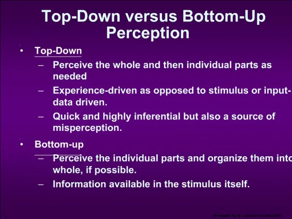
Top-down and Bottom-up Processes. What Constitutes a Top-down Process?. Adding a layer of another material over the entire wafer and patterning that layer through photolithography (??). Patterning bulk silicon by etching (??) away certain areas. www.nanoscience.at/ aboutnano_en.html.

E N D
What Constitutes a Top-down Process? • Adding a layer of another material over the entire wafer and patterning that layer through photolithography (??). • Patterning bulk silicon by etching (??) away certain areas. www.nanoscience.at/ aboutnano_en.html
Top-Down Approach • Uses the traditional methods to pattern a bulk wafer. • Is limited by the resolution of lithography. http://pages.unibas.ch/phys-meso/Education/Projektstudien/Lithographie/Litho-M1-Lithography.html
Problems with the Top-down Process • Cost of new machines and clean room environments grows exponentially with newer technologies. • Physical limits of photolithography are becoming a problem. • With smaller geometries and conventional materials, heat dissipation is a problem. http://www.cit.gu.edu.au/~s55086/qucomp/gifs/intro.moore1.gif
Bottom-Up Approach • The opposite of the top-down approach. • Instead of taking material away to make structures, the bottom-up approach selectively adds atoms to create structures. http://idol.union.edu/~malekis/ESC24/KoskywebModules/sa_topd.htm
The Ideas Behind the Bottom-up Approach • Nature uses the bottom up approach. • Cells • Crystals • Humans • Chemistry and biology can help to assemble and control growth.
Top-down Versus Bottom-up Top Down Process Bottom Up Process Start with bulk wafer Start with bulk wafer Alter area of wafer where structure is to be created by adding polymer or seed crystals or other techniques. Apply layer of photoresist Expose wafer with UV light through mask and etch wafer Grow or assemble the structure on the area determined by the seed crystals or polymer. (self assembly) Etched wafer with desired pattern Similar results can be obtained through bottom-up and top-down processes
Why is Bottom-Up Processing Needed? • Allows smaller geometries than photolithography. • Certain structures such as Carbon Nanotubes and Si nanowires are grown through a bottom-up process. • New technologies such as organic semiconductors employ bottom-up processes to pattern them. • Can make formation of films and structures much easier. • Is more economical than top-down in that it does not waste material to etching.
Where does the inspiration comes from ? And the answer is nature……………….. 1. Lotus leaf: 2. Gecko
Self Assembly • The principle behind bottom-up processing. • Self assembly is the coordinated action of independent entities to produce larger, ordered structures or achieve a desired shape. • Found in nature. • Start on the atomic scale.
Applications of Bottom-Up Processing • Self-organizing deposition of silicon nanodots. • Formation of Nanowires. • Nanotube transistor. • Self-assembled monolayers. • Carbon nanotube interconnects. http://web.ics.purdue.edu/~mmaschma/bias_image_gallery1.htm
Challenges for the Bottom-Up Approach • Making sure that the structures grow and assemble in the correct way. • Forming complex patterns and structures using self assembly. • Contamination has a significant impact on devices with such small geometries. • Fabricating robust structures.
Strategies for Bottom-Up Processing • Combination of top-down and bottom-up processes to simplify construction. • Use catalysts and stresses to achieve more one-directional growth. http://www.isnm2005.org/_metacanvas/attach_handler.uhtml?attach_id=296&content_type=application/pdf&filename= Paper%2036.pdf
Outcomes of Top-down and Bottom-Up Processes http://www.imec.be/wwwinter/business/nanotechnology.pdf
Advancements Made so Far • Carbon nanotube transistor (Stanford U.) • Organic monolayers for organic transistor (Yale U.) • Nanotube based circuit constructed (IBM) • Nanomotors and gears created (NASA) http://snf.stanford.edu/Education/Nanotechnology.SNF.ppt
Nanodots Process for making nanodots • Apply layer of self-assembled polymer film. • Grow layer of desired material to create nanodot. Polymer template for nanodot http://news.bbc.co.uk/1/hi/sci/tech/33010241.stm 65 billion nanodots per square cm
Nanodots Each nanodot can hold one bit of information. 13 nm high 80 nm wide 10 Trillion dots per square inch. Self Assembled Nanodots http://physics.nist.gov/Divisions/Div841/Gp3/Projects/Atom/atom_dots_proj.html