Download
1 / 24
250 likes | 396 Vues
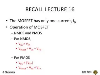
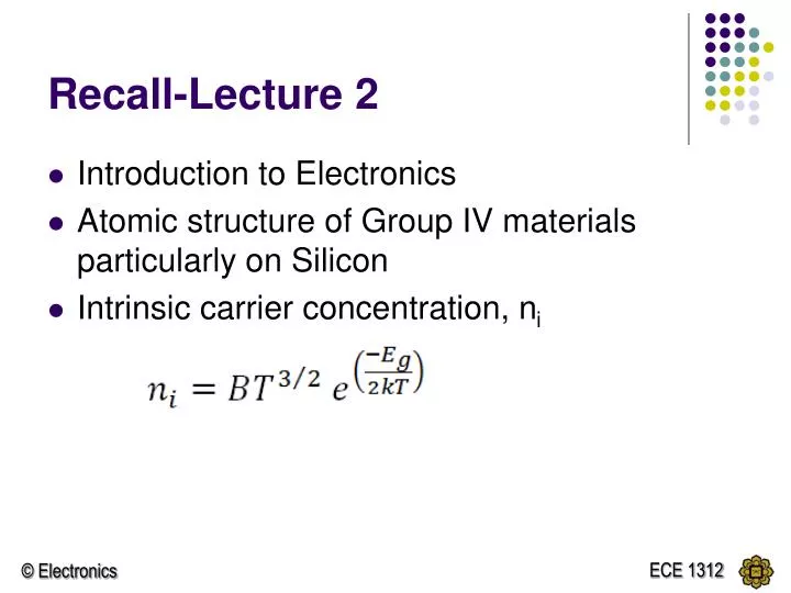
Recall-Lecture 2 . Introduction to Electronics Atomic structure of Group IV materials particularly on Silicon Intrinsic carrier concentration, n i. Recall-Lecture 2 . Extrinsic semiconductor N-type – doped with materials from Group V Majority carriers = electron

E N D
Recall-Lecture 2 • Introduction to Electronics • Atomic structure of Group IV materials particularly on Silicon • Intrinsic carrier concentration, ni
Recall-Lecture 2 • Extrinsic semiconductor • N-type – doped with materials from Group V • Majority carriers = electron • P-type – doped with materials from Group III • Majority carriers = holes • concentration of carriers in doped semiconductors • nopo = ni2
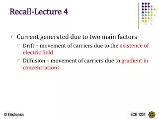
Drift and Diffusion Currents • Current Generated by the movement of charged particles (negatively charged electrons and positively charged holes). • Carriers The charged electrons and holes are referred to as carriers • The two basic processes which cause electrons and holes move in a semiconductor: • Drift- the movement caused by electric field. • Diffusion- the flow caused by variations in the concentration.
E I Vdn e Drift Currents • Drift Current Density (n-type semiconductor) • An electric field E applied to n-type semiconductor with a large number of free electrons. • Produces a force on the electrons in the opposite direction, because of the electrons’ negative charge. • The electrons acquire a drift velocity, Vdn (in cm/s): N-type
E I Vdp p Drift Currents • Drift Current Density (p-type semiconductor) • An electric field E applied to p-type semiconductor with a large number of holes. • Produces a force on the holes in the same direction, because of the positive charge on the holes. • The holes acquire a drift velocity, Vdp(in cm/s): P-type
Diffusion Current • The basic diffusion process • Flow of particles from a region of high-concentration to a region of low-concentration. • The movement of the particles will then generate the diffusion current
n-type versus p-type • In n-type - the electrons are the majority carriers and holes are the minority carriers. • In p-type - the holes are called the majority carriers and electrons are the minority carriers.
Creates a charge separation that sets up electric field, E Electron diffusion Hole diffusion - - - - - - ++ ++ ++ E The Equilibrium pn Junction • Join n-type and p-type doped Silicon (or Germanium) to form a p-n junction. p n The Electric field will create a force that will stop the diffusion of carriers reaches thermal equilibrium condition
W - - - - - - ++ ++ ++ p n E Known as space charge region/depletion region. Potential difference across the depletion region is called the built-in potential barrier, or built-in voltage: VT = kT/e • k = Boltzmann’s constant • T = absolute temperature • e = the magnitude of the electronic charge = 1 eV • Na= the net acceptor concentration in the p-region • Nd= the net donor concentration in the n-region VT = thermal voltage, [VT= kT / e] it is approximately 0.026 V at temp, T = 300 K
The Equilibrium pn Junction Example Calculate the built-in potential barrier of a pn junction. Consider a silicon pn junction at T = 300 K, doped Na = 1016 cm-3 in the p-region, Nd = 1017 cm-3 in the n-region and ni = 1.5 x 1010 cm-3. Solution
Example 2 Consider a silicon pn junction at T = 400K, doped with concentrations of Nd = 1018 cm-3 in n-region and Na = 1019 cm-3 in p-region. Calculate the built-in voltage Vbi of the pn junction, given Given B and Eg for silicon are 5.23 x 1015 cm-3 K-3/2 and 1.1 eV respectively
ANSWER • Calculation of VT = kT / e = 86 x 10-6 ( 400 ) / 1eV = 0.0344 V • Calculation of ni = BT3/2 exp ( -Eg / 2kT ) = 5.23 x 10¹⁵ ( 400 ) 3/2 exp -1.1 / 2 (86 x 10-6 ) (400) = 4.76 x 1012 cm –3 • Calculation of Vbi = VT ln ( NaNd / ni2 ) = 0.0344 ln 1018 (1019 ) / (4.76 x 10¹²)2 = 0.922V
Reverse-Biased pn Junction • +ve terminal is applied to the n-region of the pn junction and vice versa. • Applied voltage VR will induce an applied electric field EA. • Direction of the EA is the same as that of the E-field in the space-charge region. • Magnitude of the electric field in the space-charge region increases above the thermal equilibrium value. Total ET = E + EA • Increased electric field holds back the holes in the p-region and the electrons in the n-region.
Hence, no current across the pn junction. This applied voltage polarity is called reverse bias. E charge so, since there is an increase of the electric field in the depletion region, the number of charges increases too since the width of the depletion increases. Reverse-Biased pn Junction W - - - - - - ++ ++ ++ p n E - - - - - - ++ ++ ++ ET Equilibrium - - - - - - ++ ++ ++ p n Reverse Biased WR
The space charges increase with increase of reverse-bias voltage, so a capacitor is associated with the pn junction when a reverse-bias voltage is applied. The junction capacitance or depletion layer capacitance of a pn junction is Vbi EXAMPLE 2.4 Calculate the junction capacitance of a silicon pn junction diode. Consider that the diode is at room temperature (T = 300°K), with doping concentrations of cm-3 , cm-3 and let . Calculate the junction capacitance at reverse bias 3.5 V.
Forward-Biased pn Junction • +ve terminal is applied to the p-region of the pn junction and vice versa. • Direction of the applied electric field EA is the opposite as that of the E-field in the space-charge region. • The net resultis that the electric field in the space-charge region lower than the thermal equilibrium value causing diffusion of charges to begin again. • The diffusion process continues as long as VD is applied. • Creating current in the pn junction, iD.
W - - - - - - ++ ++ ++ p n E WF Forward-Biased pn Junction Equilibrium - - - - - - ++ ++ ++ p n Forward Biased Width reduces, causing diffusion of carriers current flows
Ideal Current-Voltage Relationship • So, the current iD is IS= the reverse-bias saturation current (for silicon 10-15 to 10-13 A) VT = the thermal voltage (0.026 V at room temperature) n = the emission coefficient (1 ≤ n ≤ 2)
Ideal Current-Voltage Relationship Example Determine the current in a pn junction diode. Consider a pn junction at T = 300 K in which IS = 10-14 A and n = 1. Find the diode current for vD = +0.70 V and vD = -0.70 V. Very small current
Example 2 • A silicon pn junction diode at T=300K has a reverse biased current of Is = 10-14 A. Determine the forward biased current for • VD = 0.5V • VD = 0.6V • VD = 0.7V
PN Junction Diode • The basic PN junction diode circuit symbol, and conventional current direction and voltage polarity. • The graphs shows the ideal I-V characteristics of a PN junction diode. • The diode current is an exponential function of diode voltage in the forward-bias region. • The current is very nearly zero in the reverse-bias region.
PN Junction Diode • Temperature Effects • Both IS and VT are functions of temperature. • The diode characteristics vary with temperature. • For silicon diodes, the change is approximately 2 mV/oC. • Forward-biased PN junction characteristics versus temperature. • The required diode voltage, Vto produce a given current decreases with an increase in temperature.