Download
1 / 22
230 likes | 258 Vues
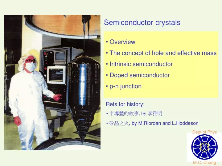
Dept of Phys. M.C. Chang. Semiconductor crystals. Overview The concept of hole and effective mass Intrinsic semiconductor Doped semiconductor p-n junction. Refs for history:. 半導體的故事, by 李雅明 矽晶之火 , by M.Riordan and L.Hoddeson. Elements. Compounds. Bonding becomes more ionic.

E N D
Dept of Phys M.C. Chang Semiconductor crystals • Overview • The concept of hole and effective mass • Intrinsic semiconductor • Doped semiconductor • p-n junction Refs for history: • 半導體的故事, by 李雅明 • 矽晶之火, by M.Riordan and L.Hoddeson
Elements Compounds Bonding becomes more ionic • (at 300K) Ge Si GaAs GaN • energy gap (eV) 0.67 (i) 1.11 (i) 1.43 (d) 3.39 (d) • lattice type Diamond Diamond Zincblend • Semiconductor is insulator at 0 K, but because of its smaller energy gap (diamond = 5.4 eV), electrons can be thermally excited to the conduction band more easily. • Si-based device can endure higher working temperature than Ge-based (75 oC) device (Si has a larger band gap) For history of semiconductor industry, see矽晶之火
Direct band gap (GaAs, GaN…) Indirect band gap (Si, Ge…) =Eg =Eg+ Direct band gap semiconductor can emit light efficiently (1μm=1.24 eV)
發明前 發明後 See Interview with Nakamura: Scientific American, July, 2000 The invention of blue-light LED GaN can emit blue light because of its large band gap (3.4 eV) • First blue-light LED: Shuji Nakamura 1989 • First blue-light laser: Shuji Nakamura 1997 中村秀二
Overview The concept of hole and effective mass Intrinsic semiconductor Doped semiconductor p-n junction
A nearly-filled band • ∴ unoccupied states behave as +e charge carriers A filled band does not carry current (Peierls, 1929) • Electric current density • For crystals with inversion symmetry, • n(k)= n(-k) • electrons with momenta ħk and -ħk have opposite velocities • no net current in equilibrium
The concept of holes (Peierls, 1929) If an electron of wavevector ke is missing, then k= -ke. Alternatively speaking, a hole with wavevector kh is produced (and kh= -ke). The lower in energy the missing electron lies, the higher the energy of the whole system. If the energy of a filled valence band is set to zero, then h k The missing electron
The concept of effective mass Near the bottom of a conduction band, the energy dispersion is approximately parabolic Reciprocal effective mass matrix The electron near band bottom is like a free electron (with m*). • For a spherical FS, m*ij=m*δij, one m* is enough. • In general, electron in a flatter band has a larger m* • Negative effective mass: • If E(k) is (e.g. top of valence band) then m*<0 • electron (-e) with negative m* = hole (+e) with positive m*
T L For ellipsoidal FS, there can be at most three different m*s Eg. the FS of Si is made of six identical ellipsoidal pockets • For Si, Eg = 1.1 eV, mL= 0.9 m, mT= 0.2 m (it’s more difficult for the electron to move along the L direction because the band is flatter along that direction)
More band structures and Fermi surfaces Common features Useful parameters mL /mT mHH/mLH Δ Si 0.91/0.19 0.46/0.16 0.044 eV GaAs 0.063 0.5/0.076 0.3 eV
Overview The concept of hole and effective mass Intrinsic semiconductor Doped semiconductor p-n junction
Density of states and carrier density • At room temperature, ε-μ >> kBT, electron density in conduction band: Top of valence band is set as E=0 • hole density in valence band:
Carrier density and energy gap Chemical potential In intrinsic semiconductor, • the density of intrinsic carriers depends only on the energy gap. The 2nd term is very small because kBT<<EG (For Si, the atom density is 5×1022cm-3.)
Impurity level: Bohr atom model • The ionized impurity atom has hydrogen-like potential, • (m m*, ε0 ε) • Dielectric constant of Si = 11.7 (Ge=15.8, GaAs=13.13) • Effective mass for Si =0.2 m • Therefore, the donor ionization energy = 20 meV. • Bohr radius of the donor electron, • For Si, it's about 50 A (justifies the use of a constant ε)
Impurity levels in Si Conduction band Valence band Energy-band point of view
The law of mass action When the doping density >> ni, we can simply ignore ni (for majority carrier). Then the density of minority carrier is determined by the law of mass-action.
Overview The concept of hole and effective mass Intrinsic semiconductor Doped semiconductor p-n junction (extra)
Equilibrium B.G. Streetman, Solid State Electronic Devices
Equilibrium With external bias Rectification B.G. Streetman, Solid State Electronic Devices