Download
1 / 25
250 likes | 384 Vues
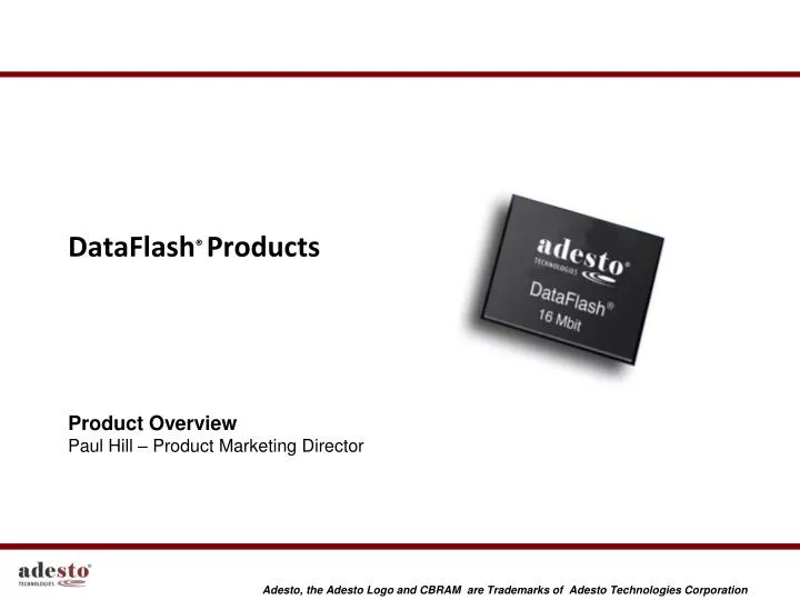
DataFlash ® Products. Product Overview Paul Hill – Product Marketing Director. The DataFlash ® Concept. DataFlash ® Product Line Evolution…. 15 years of support and backwards compatibility. 2002-2007 AT45DBxxxB Legac y. 2007-2013 AT45DBxxxD Current. 2013+ AT45DBxxx E

E N D
DataFlash® Products Product Overview Paul Hill – Product Marketing Director
DataFlash® Product Line Evolution… 15 years of support and backwards compatibility 2002-2007 AT45DBxxxB Legacy 2007-2013 AT45DBxxxD Current 2013+ AT45DBxxxE Next Generation • Smallest Page Sizes • Dual SRAM Buffers • Command Rich I/F • Serial E² Emulation • Page Erase / Page Write • Flexible Sector Protection • Any Sector Lockdown • 128Byte Security Register • Ind. Std. Device ID • Byte Write Capability • Dual/Quad IO Interfaces • Low-power Modes • 1.65V & 2.3V Operation 3
The DataFlash®‘E’ Series Revolution! • Read While Write Capability • Erase-Program-Suspend-Resume NEW E Series Features • Sector Security • Flexible Non-Vol. • Sector Protection Extended VCC Range • 1.65V – 3.6V • 2.3V – 3.6V NOR FLASH MEMORY ARRAY Small Page Array Architecture • Higher Performance • 85Mhz SPI Clock RESET • Sector Lockdown • Make any Sector • Perm. Read Only PAGE SIZE = BUFFER SIZE WP Low Power Read • Lower Power Read • <20MHz Dual SRAM Buffers • Each SRAM Buffer • = One Page Size. BUFFER 2 BUFFER 1 SCK CS I/O INTERFACE • Byte Write Capability • Byte write Option • without Pre-Erase • 3% More Memory • Additional NVM • Storage Capacity • Enhanced Interface Options • RapidS, Dual IO, Quad IO & Rapid4 SI SO • Zero Power Mode • Ultra Deep Power • Down Mode @ 300nA • Software RST CMD. • Built In Device • Reset command 4
DataFlash® Value Proposition.... DataFlash contributes to an overall lowersystem cost
DataFlash® SRAM Buffer BenefitsAdditional System SRAM FLASH MEMORY ARRAY PAGE BUFFER 1 BUFFER 2 I/O INTERFACE SI • Use the DataFlash internal SRAM Buffers as EXTRA system RAM • Temporarily off-load data from the MCU RAM to the DataFlash RAM Buffers SRAM Utilization SYSTEM SRAM ALERT
DataFlash®SRAM Buffer BenefitsContinuous - Faster Programming and Data Streaming FLASH MEMORY ARRAY FLASH MEMORY ARRAY PAGE PAGE TRANSFER DATA FROM BUFFER TO MAIN MEMORY BUFFER 1 BUFFER 2 BUFFER 1 BUFFER 2 WRITE DATA INTO BUFFER WRITE DATA INTO BUFFER I/O INTERFACE I/O INTERFACE SI SI Ideal for Data Streaming and Quickly Writing Large Blocks of Code or Data • Step 2 • 1. Stream Data to Buffer 2 • Start Buffer Programming • Repeat Step 1 • Step 1 • Stream Data to Buffer 1 • Start Buffer 1 Programming
Benchmark ResultsSingle Buffer versus Dual Buffer Programming Note 1: Time to erase and program. 4096 bytes (1 block in Serial Flash) vs. 1056 bytes (1 page in DataFlash) Setup: AT91SAM9XE-EK, at91lib version 1.5
DataFlash®SRAM Buffer Benefits Endurance Enhancement Write 100 times to the buffer & once to the Flash = 100:1 Endurance Improvement FLASH MEMORY ARRAY • Write Frequently into BUFFER A & B • No Endurance Limitation • Uses Less Energy • Is much faster • Write Buffer Data occasionally into Memory • Reduces the # Program cycles • Extends the life of the memory • Avoids Complex Software Wear Leveling & Endurance Enhancement Algorythms (ECC) PAGE WRITE BUFFER DATA INTO MEMORY BUFFER 1 BUFFER 2 WRITE DATA INTO BUFFERs I/O INTERFACE SI
DataFlash®SRAM Buffer Benefits Power Fail Management Enhancement FLASH MEMORY ARRAY • Use BUFFER 1 for frequent programming • No endurance limitation • Uses less energy than programming to Flash memory every time • Is much faster than writing to Flash every time allowing the CPU to shut-down faster • Use BUFFER 2 for Power Fail Data • Regularly upload power fail data to Buffer B • Initiate Buffer B programming immediately on power fail • Reduces the CPU overhead in the event of a power fail. PAGE WRITE BUFFER DATA INTO MEMORY BUFFER 1 BUFFER 2 WRITE DATA INTO BUFFERs I/O INTERFACE SI
DataFlash® Intelligent Internal AlgorithmsEnable “Offloading” CPU Tasks: More CPU Cycles Available for Metering Functions • DataFlash • The first Serial Flash Memory to Support a BYTE WRITE operation • Requires NO CPU override, Management or support • Enable DataFlash to pick up where Serial E² Finishes. Traditional Flash DataFlash “D” DataFlash “E” Copy 4KB block to CPU SRAM Memory Page to Buffer Transfer Issue 0x58h Cmd. with 1-PageN Bytes Erase 4KB Block in Memory Modify Buffer Contents Poll Device Page to Memory Program Erase Done? Modify Data in System SRAM Poll Device Program 4KBytes SRAM Data 256byte / cycle PGM. Done? 11
Program Erase Suspend / Resume • Program Erase Suspend / Resume • This pair of commands will allow the application to read data from the memory array even during a Programming or Erase operation • Traditionally the application would have to wait for the end of the Flash memory programming or erase cycle first before the next read operation can begin. • It can be considered to be a Program or Erase PAUSE Command
Benchmark ResultsCode Efficiency and CPU Overhead A 256 Byte Read Modify Write Programming Operation Code Example Benchmark • External. SRAM • ZERO BYTES • External. SRAM • 4K BYTES • CPU RAM/STACK • 60 Bytes • CPU RAM/STACK • 56 Bytes • Flash Code Size: • 300 Bytes • Flash Code Size: • 560 Bytes Note 1: Time to erase and program. 4096 bytes (1 block in Serial Flash) vs. 1056 bytes (1 page in DF) Setup: AT91SAM9XE-EK, at91lib version 1.5 13
Benchmark ResultsProgramming Execution Times Note 1: Time to erase and program. 4096 bytes (1 block in Serial Flash) vs. 1056 bytes (1 page in DataFlash) Setup: AT91SAM9XE-EK, at91lib version 1.5 14
DataFlash®Low Power Capabilities“Ultra Deep Power Down” Enables Power Saving with Less Components • Traditional Solution • Control VCC with a LDO / FET • True Zero Power • LDO / FET Costs ~$0.05 • Need 1 Dedicated MCU GPIO Pin LDO / FET VCC SO SO SI SI GPIO GND GND SCK SCK VCC VCC /RST /RST /WP /WP /CS /CS DataFlash “E” Issue 0x79h Cmd. Ultra-Deep PD Ultra Deep Power Down Command Done • DataFlash Solution • Control Vcc via UDPD Command • Typ ~400nA current • No LDO / FET Required • Requires No MCU GPIO VCC
DataFlash®Low Power CapabilitiesExtended Vcc Range (1.65 to 3.6V) enables longer battery life and cost savings 2.7V 2.5V 2.3V 1.65V – 3.6V Amp-Hours 113% 413% More Battery Life Note: Battery discharge data from www.powerstream.com/AA-tests.htm 1073% More Battery Life
DataFlash®Low Power CapabilitiesExtended Vcc Range (1.65 to 3.6V) Enhanced Power Fail Performance 2.7V 2.5V 2.3V 1.65V – 3.6V Time Power Fail Alert CPU Executing Shut Down Sequence Last Minute Power Fail Data Program Operation Initial Page-Program (Pre-Stored Data) DataFlash can operate for Longer due to the wide operating VCC range Note: Battery discharge data from www.powerstream.com/AA-tests.htm
Software Reset • This command will allow the application to force the DataFlash to RESET • A Software Reset is essential when considering eXecute-in-Place (XiP) applications or critical Data Storage events such as Power Fail • Kill any Program Erase Operation. • Read from other parts of the array • Terminate the Erase-Program-Resume-Suspend cycle • Spec • Software Reset time ~30us plus CPU time
DataFlash® Security FeaturesSector Protection Mechanism Independent Sector Protection Write-Protect any sector at any time Write Protect Status is non-volatile Benefit =Critical S/W updates Permanent Sector Lockdown Make any sector Read Only. Once locked the sector cannot be erased or re-programmed Benefit =Boot/Recovery/Security S/W Lockdown Command FREEZE (DISABLE) Prevent further permanent sector lockdown operations Remaining sectors can no longer be permanently locked down. Does not inhibit Independent sector protection Benefit =Malicious Hacks Sector Security Options Sector 0a (8 Pages) Sector 0b (248 Pages) Sector 1 (256 Pages) Sector 2 (256 Pages) Sector and Page Architecture Diagram . . . . . . Sector 15 (256 Pages) Example AT45DB161D/E
DataFlash®Security FeaturesUnique Device ID • Enhance System Security & Electronic Inventory Control • The Security Register Is Divided into Two parts • The 1st 64 bytes • Can be programmed by the customer and also securely locked. • Once programmed it Cannot be Erased / Re-programmed • The 2nd 64 bytes • Are Factory Programmed with a Unique S/N • The S/N can provide traceability to LOT#, Wafer# and DIE XY Level
DataFlash® Enhanced SecuritySimplified Anti-Tamper Mechanism using the Unique ID Data Flash Contains a copy of the CPU UID in Secure LOCKED OTP MEMORY • @ Power-Up, MCU reads the DF UID and compares to stored value in Embedded Flash • MCU reads its own UID and compares to store value in DF • If either result = False System error is reported as possible tamper event • Cycle is repeated during normal system operation DataFlash Communication Processor 64 Byte UID LCD 32-bit MCU I/O Link MCU Embedded Flash Breaker Embedded CPU S/N or UID Line Operated & Battery Back-Up 16bit / 32bit MCU Contains a copy of the DataFlash UID in the embedded secure MCU Flash External SRAM 24-bit ADC & Precision Energy Metering IC Smart Meter Sub System
DataFlash® Quality and Performance Inside.....Enhanced Intelligent Adaptive Embedded Programming Algorithms DataFlash PRGM. Cycle Adaptive Algorithm Program all ‘1’s to ‘0’s Program / Erase Pulse ‘Balance’ Cycle Adaptive Algorithm Compare Cell Margin > Buffer Erase All Bits to ‘1’ Done ‘Erase’ Cycle Adaptive Algorithm Program Buffer Contents to NVM Array ‘Program’ Cycle Adaptive Algorithm Done
The DataFlash® Message And Value Proposition • Dual on chip SRAM Buffers • Page Write / Page Erase & Byte Write capability • 3% More Memory Less System Complexity • Command Rich / Command Driven Architecture • Lower CPU Overhead & Smaller S/W Footprint • Fewer System Resources Higher System Performance • Ultra Deep Power Down Mode & Low Power Read • Wide Vcc Range for fewer LDOs & Greater Cell Life / Smaller Cells • Lower CPU Power Signature Better Energy Management • Individual Sector Lockdown • Individual Sector Protection • Sector Lockdown Freeze Better S/W & Data Security Contributes to Improved System Performance, Efficiency & Lower Total System Cost DataFlash® 25