Download
1 / 20
200 likes | 308 Vues
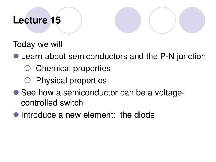
Lecture 15. Today we will Learn about semiconductors and the P-N junction Chemical properties Physical properties See how a semiconductor can be a voltage-controlled switch Introduce a new element: the diode. Si. Si. Si. Si. Si. Si. Si. Si. Si. Si. Si.

E N D
Lecture 15 Today we will • Learn about semiconductors and the P-N junction • Chemical properties • Physical properties • See how a semiconductor can be a voltage-controlled switch • Introduce a new element: the diode
Si Si Si Si Si Si Si Si Si Si Si Semiconductors: Chemical Structure Start with a silicon substrate (block of silicon). Silicon has 4 valence electrons, and therefore a “lattice” structure: Each atom bonds with 4 neighbors. No free electrons (poor conductor) unless you heat it up (semi conductor). Other Group IV elements can be used for substrate, but they are harder to come by (carbon lattice for instance…)
Si Si Si Si Si Ga Si Si Si Si Si Doping: p-type Make silicon a better conductor by adding Group III or Group V elements: process called doping Add Group III elements like gallium or indium to substrate to get p-type material. Note that the Ga atom has only 3 valence electrons with which to bond; missing bond is called a hole. Material is electrically neutral! Equal number of protons and electrons! hole
Si Si Si Si Si As Si Si Si Si Si e Doping: n-type Add Group V elements like arsenic or phosphorus to substrate to get n-type material. Note that the As atom has 5 valence electrons; it has an unbonded electron. Material is electrically neutral! Equal number of protons and electrons!
e e e h h h e e e h h h p-type extra holes n-type extra e- aluminum e e e h h h P-N Junction: The Basis For Electronics Put p-type and n-type material together: Essential Property: Make current flow (or not flow) by applying electric field (voltage) to metal ends. - + We call this device a diode. “Voltage Controlled Switch”
Diffusion and Drift Electrons can be moved by two types of attraction: • Diffusion Electrons will move from an area of greater concentration (extra free electrons, e.g. n-type) to an area of lesser concentration (holes to fill, e.g. p-type) • Drift Electrons will move according to an applied electric field, toward a region of higher potential (voltage)
e e e h h h h h - + e e + e e e e h h h h h - e e e h h h + e e h h - e Physics of P-N JunctionCase: Open Circuit Diffusion moves free electrons from n-type to holes in p-type. “Uncovered” protons are left in n-type, extra electrons in p-type. a n-type p-type n-type p-type depletion region Area near p-n junction now has no charge carriers (free electrons or holes): called depletion region
+ e e h h - + e e h h - + e e h h - V Physics of P-N JunctionCase: Open Circuit E The charged atoms in the depletion region create an electric field, and thus a difference in electric potential. n-type p-type depletion region When the potential drop becomes steep, the free electrons no longer cross, since electrons do not want to go to an area of lower potential. Drift takes over, and the electrons stay put. dist from junction
h h - + e e h h - + e e h h - + e e Physics of P-N JunctionCase: Short Circuit Is there a current when I short a diode? Is KVL violated? NO. n-type p-type At metal-semiconductor junction, potential changes to balance device. Electrons in metal can redistribute easily to do this. V metal contact metal contact dist from junction
p-type n-type – – e + + – – e + + h – – e + + h h depletion region (no free e, h) – + VS > 0 metal contact V VS dist from junction metal contact Physics of P-N JunctionCase: Reverse Bias A diode is in reverse bias mode when the + (p-type) terminal is at a (moderately) lower potential than the – (n-type) terminal. Electrons bunch up by positive metal contact, but few cross through wire because of potential drop between contacts. A tiny “leakage current” flows due to these few stray electrons, but basically zero current flow.
h h h – + metal contact V VS dist from junction Physics of P-N JunctionCase: Reverse Breakdown p-type n-type When the diode + terminal is at a much lower potential than the - terminal, reverse breakdown occurs. The potential rise across the junction becomes so great that electrons from the p-type material travel across the rise. The rise has to be great enough to break the electrons out of their chemical bonds in the p-type material. – – e + + e – – e + + e – – e + + depletion region (no free e, h) VS > VZK metal contact Breakdown when V > VZK “Zener knee”
- + FYI: Zener Diodes • There are diodes called Zener diodes that are designed to operate in reverse breakdown. • The voltage across the diode in the reverse breakdown mode is about constant, as once the voltage gets past VZK, the depletion layer does not really increase—the current increases dramatically (also known as avalanche current). • As the reverse voltage is increased, there will be a limit to the current flow: reverse saturation current • A Zener diode is used to regulate voltage within a circuit, since it provides about the same voltage (VZK) for a whole range of reverse current conditions. • Zener diodes can be obtained for a variety of VZK values, anywhere from 0.5 V to 200 V.
– + metal contact V metal contact dist from junction VS Physics of P-N JunctionCase: Forward Bias The voltage source in this orientation makes the drop across the junction less steep. If VS is greater than the diode forward voltage parameter VF, electrons are willing to go over shallow voltage drop to fill holes. p-type n-type – + e e h – + – h e + VS > VF Electrons flow across junction and combine with holes. The need to redistribute charge at metal ends ensures continuous supply of electrons and holes. Continuous current flow!
FYI: Diodes in Forward Bias • When the voltage across the forward-biased diode is increased past VF, the current increases dramatically. • As the forward voltage is increased, there will be a limit to the current flow: saturationcurrent • When operating in forward-bias mode in a circuit, diode voltage is nearly constant (equal to VF). A voltage around VF occurs for a whole range of forward current conditions. • Many diodes have a VF of 0.6 to 0.7 V, but light emitting diodes (LED’s) often have higher VF values. An LED emits light when it is forward biased.
I I + _ Reverse bias Reverse breakdown Forward bias V V VF VZK Diode I-V Relationship • In digital circuits, P-N junctions are operating in the reverse bias or forward bias region. • To analyze the diode in a circuit, we will use mathematical approximations to the curve above, focusing on this region. • We will have various levels of detail to choose from, and the model we choose will depend on the level of accuracy desired.
I + _ V Ideal Diode Model I I • Diode either has negative voltage and zero current, or zero voltage and positive current. No possibility of positive voltage! • Diode behaves like a switch: open in reverse bias mode, closed (short circuit) in forward bias mode • Open the switch by applying negative voltage, close switch by applying zero voltage: turn current on/off via applied voltage Forward bias + _ V Reverse bias V
I + _ V Large-Signal Diode Model I I + • Diode either has voltage less than VF and zero current, or voltage equal to VF and positive current. • Diode behaves like a voltage source and switch: open in reverse bias mode, closed in forward bias mode. • This model is slightly more accurate than the ideal model, taking VF into account. Forward bias + - VF V Reverse bias V VF -
I + _ V Small-Signal Diode Model I I + • Diode either has voltage less than VF and zero current, or voltage greater than VF and positive current increasing with V. • Diode behaves like a voltage source, resistor and switch: open in reverse bias mode, closed in forward bias mode. • This model takes into account the fact that current increases slightly as forward voltage increases. + - slope = 1/RD VF Forward bias Reverse bias V RD V VF -
I + _ V Realistic Diode Model I • VT is “thermal voltage”: VT = (kT)/q ≈ 0.026 V @ 300oK • q is electron charge in C, k is Boltzmann’s constant, and T is the operating temperature in oK • I0 is a diode parameter (very small number, 10-15…) • One equation for both forward bias and reverse bias • You might need a computer to solve the nonlinear equation this model can create! V
Notes on Use of Models • Most of the models described are piecewise defined: • One function for reverse bias • Another for forward bias • You will need to: • “Guess” that diode is reverse (or forward) biased • Solve for V, I according to your guess • If this results in an impossibility, guess again • Rarely, both guesses may lead to impossibility. • Use a more detailed model