Download
1 / 27
900 likes | 2.01k Vues
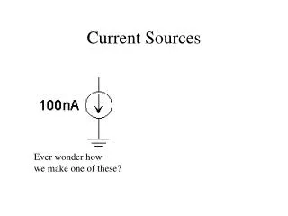
CURRENT SOURCES, CURRENT SINKS AND CURRENT MIRRORS. CURRENT SINKS AND SOURCES Characterization of Current Sinks and Sources: Minimum voltage (V MIN ) across sink or source for which the current is no longer constant.

E N D
CURRENT SOURCES, CURRENT SINKS AND CURRENT MIRRORS
CURRENT SINKS AND SOURCES • Characterization of Current Sinks and Sources: • Minimum voltage (VMIN) across sink or source for which the current is no longer constant. • Output resistance which is a measure of the flatness of the current sink or source.
Increasing the output impedance ROUT of a Current Source
If the devices are matched If VDS1 = VDS2 then
This modification to the Simple Current mirror does ensure an increased output impedance, but does not ensure VDS1 = VDS2. Vmin obtained in this configuration is the sum of the voltage, VDS1(sat) and VDS3(sat), the minimum drain to source voltage required to keep M3 and M1 in saturation. Defining VON = VGS – VTH, and assuming that all transistors have same W/L ratio, we have VDS1 = VGS1 = VON + VTH and VDS3(min) = VON and Vmin = 2VON + VTH.
REGULATED CASCODE CURRENT MIRROR If all transistors have the same size, VGS2 = VDS1 = VGS = VDS4, giving us a very good match in mirroring.
CURRENT MIRROR WITH LOW Vmin and GOOD MIRRORING PROPERTY We see that in the Cascode Current Mirror, the voltage VGG2 was obtained as 2VGS and hence we had a Vmin of 2VGS – VTH = 2VON +VTH. However if we can obtain VGG2 = 2VON + VTH, Vmin can be reduced to 2VON.