Download
1 / 14
140 likes | 234 Vues
Fabrication of oxide nanostructure using Sidewall Growth. 田中研 M1 尾野篤志. Background strongly correlated electron system( 強相関電子系 ) in nanosize. 100nm. 100nm. 100nm. 100nm. 100nm. (La, Pr,Ca ) MnO 3 film STM image. VO 2 film SNIM image. LPCMO. VO 2. Metal. Ferromagnetic.

E N D
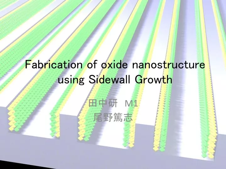
Fabrication of oxide nanostructure using Sidewall Growth 田中研 M1 尾野篤志
Backgroundstrongly correlated electron system(強相関電子系) in nanosize 100nm 100nm 100nm 100nm 100nm (La, Pr,Ca)MnO3 film STM image VO2 film SNIM image LPCMO VO2 Metal Ferromagnetic Insulator Anti-Ferromagnetic 500nm M. Fäth et al, Science 285 (1999)1540 M. M. Qazilbashet al, Science 318 (2007) 1750,
Backgroundstrongly correlated electron system(強相関電子系) in nanosize • Nanostructure lead to sharp phase transition Insulator Metal 500nm (La, Pr,Ca)MnO3 film 1μm 500nm Y. Yanagisawaet al Appl. PHYSICS LETTERS 89 (2006)253121 Charge Ordering InsulatorFerromagnetic metal Nano-structure fabrication technique Dimension-control Future advanced nano-device Size-control
Fabrication of nanostructureTop down and Bottom up Top down Technique Bottom up Technique Accumulate atoms by deposition For example ―Pulsed Laser Deposition ―Sputtering Deposition • Figure materials finely For example ―Nano Imprint Lithography ―AFM Lithography
Our nanostructure fabrication methodCombination of Top down and Bottom up Top Down Bottom up Pulsed Laser Deposisiton • Nano Imprint Technology
Purpose- Fabrication of oxide nanostructures and evaluation of their properties- • Establishment of fabrication method ZnO nanobox • Measurement of their physical properties • Application for devices ZnO: Semiconductor, Optical Device Amorphous @RT ⇒ Crystal @HT
Fabrication of the nanostructure Patterning by NIL ② Depositon using Sidewall growth ③ Removing patterns (Ion milling and Cleaning) ④ Crystallization by annealing ⑤ Measurement of their physical properties
Experimental method • Deposition on Plane Substrate 1-1. Control thin film’s thickness 1-2. Optimize crystallization condition by annealing • Deposition on Nano-pattaerne substrate ― Fabricate ZnO nanobox using sidewall growth Deposition@ Room temperature
Result1-1: Deposition of ZnO time-dependency of sidewall thickness I measured thin films’ thickness ZnO deposition: PLD method Substrate: Si(001) PO2=1.0×10⁻²Pa Deposition time: 30-120min. Evaluation method: Atomic Force Microscopy Thickness[nm] d=1.30t d: film’s thickness (nm) t: deposition time (min) Film’s thickness∝Sidewall’s thickness Deposition time [min.] Sidewall thickness : controllable
Result1-2: Crystallization condition Optimize the condition of Crystallizing ZnO Intensity (a.u.) Annealing temperature: 550-950 ℃ Evaluation method: X-ray Diffraction 2θ [°] • by Annealing • ZnO crystallization: higher than 550℃
Result2: Fabrication of ZnO nano-boxEvaluation method: Scanning Electron Microscopy Polymers on substrate ZnO-deposited substrate 45nm 1μm 500nm Ion Milling Acetone cleaning 1μm 1μm
Summary • I succeeded in fabrication of ZnO nanobox by the combination Top down (imprint) and Bottom up (PLD) technique. • The side wall thickness was45nm. • I need to improve the accuracy and responsibility. This technique can be applied for another system. Various patterns can be formed.
Example of various patterns Examples of the various patterns: Mo, Au 200 nm 200 nm N.-G. Cha et al. Nanotechnology 20 (2009) 395301 150 nm 150 nm 100 nm 60nm 2 µm
Next Step ―I am trying to fabricate Fe3-xZnxO4 nanowire MagneticField MagneticField 500nm 50nm!! Y. Yanagisawaet al Appl. PHYSICS LETTERS 89 (2006)253121 FZO Strongly correlated electron system Ferromagnetic semiconductor @ room temperature Spintronics MReffect ⇒ MRAM, Spin FET, …