Download

1 / 48
520 likes | 840 Vues
Microscopy and Surface Analysis 1. Lecture Date: March 11 th , 2008. Reading Assignments for Microscopy and Surface Analysis. Skoog, Holler and Nieman, Chapter 21, “Surface Characterization by Spectroscopy and Microscopy”

E N D
Microscopy and Surface Analysis 1 Lecture Date: March 11th, 2008
Reading Assignments for Microscopy and Surface Analysis • Skoog, Holler and Nieman, Chapter 21, “Surface Characterization by Spectroscopy and Microscopy” • Hand-out Review Article: R. J. Hamers, “Scanned Probe Microscopies in Chemistry,” J. Phys. Chem., 1996,100, 13103-13120.
Microscopy and Surface Analysis • Microscopic and imaging techniques: • Optical microscopy • Confocal microscopy • Electron microscopy (SEM and TEM, related methods) • Scanning probe microscopy (STM and AFM, related methods) • Surface spectrometric techniques: • X-ray fluorescence (from electron microscopy) • Auger electron spectrometry • X-ray photoelectron spectrometry (XPS/UPS/ESCA) • Other techniques: • Secondary-ion mass spectrometry (SIMS) • Ion-scattering spectrometry (ISS) • IR/Raman methods
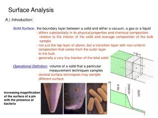
Why Study Surfaces? • Surface – the interface between two of matter’s common phases: • Solid-gas (we will primarily focus on this) • Solid-liquid • Solid-solid • Liquid-gas • Liquid-liquid • The majority of present studies are applied to this type of system, and the techniques available are extremely powerful • The properties of surfaces often control chemical reactions
Microscopy • Why is microscopy useful? What can it tell the analytical chemist? • Sample topography • Structural stress/strain • Electromagnetic properties • Chemical composition • Plus - a range of spectroscopic techniques, from IR to X-ray wavelengths/energies, have been combined with microscopy to create some of the most powerful analytical tools available…
Imaging Resolution and Magnification • Some typical values for microscopic methods:
Optical Microscopy - History • An ancient technique – the lens has been around for thousands of years. Chinese tapestries dating from 1000 B.C. depict eyeglasses. • In 1000 A.D., an Arabian mathematician (Al Hasan) made the first theoretical study of the lens. • Copernicus (1542 A.D.) made the first definitive use of a telescope. • As glass polishing skills developed, microscopes became possible. John and Zaccharias Jannsen (Holland) made the first commercial and first compound microscopes. • Then came lens grinding, Galileo, the biologists, and many great discoveries….
Modern Optical Microscopy in Chemistry • As optical microscopy developed, the compound microscope was applied to the study of chemical crystals. • The polarizing microscope (1880): can see boundaries between materials with different refractive indices, while also detecting isotropic and anisotropic materials. http://www.microscopyu.com/articles/polarized/polarizedintro.html
Optical Microscope Design • Microscope design has not changed much in 300 years • But the lenses are more perfect – free of abberations • Objective lenses are characterized NA (numerical aperature) • The numerical aperture of a microscope objective is a measure of its ability to gather light and resolve fine specimen detail at a fixed object distance • Large NA = finer detail = better light gathering Diagram from Wikipedia (public domain) http://www.microscopyu.com/articles/polarized/polarizedintro.html
The Diffraction Limit • The image of an infinitely small point of light is not a point – it is an “Airy” disk with concentric bright/dark rings Airy disk • The minimum distance between resolved point objects of equal intensity is the “Airy” disk radius (rairy), since resolution of a conventional optical microscope is limited by Fraunhofer diffraction at the entrance aperture of the objective lens Resolved Not resolved http://www.cambridgeincolour.com/tutorials/diffraction-photography.htm, http://www.olympusmicro.com/primer/java/mtf/airydisksize/ See Y Garini, Current Opinion in Biotechnology 2005, 16:3–12
The Diffraction Limit • Traditional optical microscopy is known as “far-field” microscopy. Its lateral resolution is limited to ~200 nm. • The need for the light-gathering objective lens and its aperture in a conventional microscope leads to a diffraction limit • Newer techniques make use of “near-field” methods to overcome the diffraction limit. A fiber tip with an aperture <100 nm is scanned over a sample (forming the basis of techniques like NSOM/SNOM – the scanning near-field optical microscope). • NSOM is now being using in conjunction with AFM – to study “nano-phototonics” • Resolution now down to ~30 nm
Confocal Scanning Microscopy • Confocal imaging (or confocal scanning microscopy, CSM) was first proposed by Marvin Minsky in 1957. • Confocal imaging: A technique in which a single axial point is illuminated and focused at a time. The light reflected (or produced e.g. by fluorescence) is detected for just that point. Light from out-of-focus areas is suppressed. A complete image is formed by scanning. • Advantages over conventional optical microscopy: • Greater depth of field from images • Images are free from out-of-focus blur • Greater signal-to-noise ratio (for a spot – but images take time!) • Better effective resolution (diffraction limit) M. Minsky, “Memoir on inventing the confocal scanning microscope”. Scanning, 1988, 10, 128-138.
Confocal Scanning Microscopy: Imaging Types • One type of imaging “mode” is stage or object scanning: • A more modern “mode” is laser scanning: • Nipkow disks can be used for studying moving samples • disks with staggered holes – block all but a certain lateral portion of the sample beam
Laser Confocal Scanning Microscopy • Laser confocal scanning (LSCM) is the most common type of CSM • Applications: • Biochemistry (including fluorescence probes) • Materials science • Can be used with a fluorescent dye to stain biological samples Diagram from http://www.cs.ubc.ca/spider/ladic/images/system.gif
Laser Confocal Scanning Microscopy • A complete LCSM system: Diagram from http://www.cs.ubc.ca/spider/ladic/images/system.gif
Laser Confocal Scanning Microscopy • LCSM is often combined with fluorometry or with Raman • For fluorometry, there are numerous LCSM fluorophores: Diagram from http://www.cs.ubc.ca/spider/ladic/images/system.gif
IR Microscopy and Spectroscopy • Most FTIR microscopes image using array detectors • IR spectra from a region are acquired at once, better S/N • However, this is at the expense of resolution (limited to ca. 10 um), in contrast with scanning techniques. Resolution in FTIR imaging is of course limited by the diffration limit, which is even worse for IR wavelengths. Figure from J. L. Koenig, S. Q. Wang, and R. Bhargava, Anal. Chem.,73, 361A-369A (2001).
IR Microscopy: Image Analysis • Extraction of data from FTIR micrographs is done by color-coding peaks based on their IR frequency (a) • Suitable IR frequencies can be chosen via a scatter plot (c) of every point in the image vs. two (or more) frequencies, followed by location of the center-of-gravity and possible statistical analysis • False color images can then be constructed (b) Figure from J. L. Koenig, S. Q. Wang, and R. Bhargava, Anal. Chem.,73, 361A-369A (2001).
IR Microscopy: Polymer Chemistry Applications • FTIR microscopy can analyze compositional differences in material science, chemical and biochemical applications • Example – the study of time-dependent processes like dissolution of a polymer by a solvent Figure from J. L. Koenig, S. Q. Wang, and R. Bhargava, Anal. Chem.,73, 361A-369A (2001).
IR Microscopy: Polymer Chemistry Applications • A complex, solvent-dependent dissolution, diffusion and molecular motion process is observed for polymers (e.g. polymethylstyrene) above their entanglement mwt: Figure from J. L. Koenig, S. Q. Wang, and R. Bhargava, Anal. Chem.,73, 361A-369A (2001).
Raman Microscopy • Raman microscopy – better inherent resolution than IR (uses lasers at shorter optical wavelengths) • Not capable of imaging (must still scan the sample) – this does have its advantages though • Often integrated with LCSM systems for combined 3D visualization and spectroscopy
Raman Microscopy: Forensic Applications • Raman microscopy has many obvious applications – one that is not so obvious is for forensic analysis of colored fibers. • The Raman spectra obtained from fibers acts as a fingerprint, and the complex spectra obtained from dye mixtures can be used to determine if two fibers are from the same origin • The individual dyes used in fabics are varied, and their ratios are especially varied (even from batch to batch!) • Competing techniques are generally destructive – e.g. LC or ESI MS on dye-containing extracts from fibers For more about forensic Raman microscopy, see: T. A. Brettell, N. Rudin and R. Saferstein, Anal. Chem.,75, 2877-2890 (2003).
Electron Microscopy (EM) • Scanning electron microscopy (SEM) – an electron beam is scanned in a raster pattern and “reflected” effects are monitored. Velcro (x35) Ice crystals optical SEM • Transmission electron microscopy (TEM) – “transmitted” electrons are monitored. Most TEM are actually scanning – STEM! • Contrast is created in a totally different manner in EM Bottom photo - http://www.mos.org/sln/sem/velcro.html Top photo - http://emu.arsusda.gov/snowsite/default.html
Electron Microscopy: Basic Design • Basic layout of an electron microscope: Electron gun (1-30 keV) Computer Magnetic lenses and scanning coils Detectors electrons photons Sample electrons Detectors
Electron Microscopy: Resolution • Why can an electron microscope resolve things that are impossible to discern with optical microscopy? • Example – calculate the wavelength of electrons accelerated by a 10 kV potential: Note: Resolution is limited by lens aberations! EM can see >10000x more detail than visible light!
Electron Microscopy: Resolution • What about relativistic corrections? The electrons in an EM can in some cases be moving pretty close to the speed of light. • Example – what is the wavelength for a 100 kV potential? Using the relativistically corrected form of the previous equation: At high potentials, EM can see atomic dimensions
Electron Microscopy: Sample-Beam Interactions • Sample-beam interactions control how both SEM and TEM (i.e. STEM) operate: • Formation of images • Spectroscopic/diffractometric analysis • There are lots (actually eight) types of sample-beam interactions (which can be confusing and hard to remember!) • It helps to classify these 8 types into two classes of sample-beam interactions: • bulk specimen interactions (bounce off sample – “reflected”) • thin specimen interactions (travel through sample- “transmitted”)
SEM: Sample-Beam Interactions Backscattered Electrons (~30 keV) • Caused by an incident electron colliding with an atom in the specimen which is almost normal to the incident electron’s path. The electron is then scattered "backward" 180 degrees. • Backscattered electron intensity varies directly with the specimen's atomic number. This differing production rates causes higher atomic number elements to appear “brighter” than lower atomic number elements. This creates contrast in the image of the specimen based on different average atomic numbers. • Backscattered electrons can come from a wide area around the beam impact point (see pg. 552 of Skoog) – this also limits the resolution of a SEM (along with abberations in the EM lenses)
SEM: Sample-Beam Interactions Secondary Electrons (~5 eV) • Caused by an incident electron passing "near" an atom in the specimen, close enough to impart some of its energy to a lower energy electron (usually in the K-shell). This causes a slight energy loss, a change in the path of the incident electron and ionization of the electron in the specimen atom. The ionized electron then leaves the atom with a very small kinetic energy (~5 eV). One incident electron can produce several secondary electrons. • Production of secondary electrons is closely linked to sample topography. Their low energy (~5 eV) means that only electrons very near to the surface (<10 nm) are detected. They also don’t suffer from the backscattered electron lateral resolution problem depicted in Fig. 21-16 of Skoog. Changes in topography in the sample that are larger than this sampling depth can change the yield of secondary electrons via indirect effects (called collection efficiencies).
Electron Microscope: Image Formation From JEOL Application Note, V. E. Robertson, ca. 1985.
SEM: Sample-Beam Interactions Auger Electrons (10 eV – 2 keV) • Caused by relaxation of an ionized atom after a secondary electron is produced. The lower (usually K-shell) electron that was emitted from the atom during the secondary electron process has left a vacancy. A higher energy electron from the same atom can drop to a lower energy, filling the vacancy. This leaves extra energy in the atom which can be corrected by emitting a weakly-bound outer electron; an Auger electron. • Auger electrons have a characteristic energy, which is unique and depends on the emitting element. Auger electrons have relatively low energy and are only emitted from the bulk specimen from a depth of several angstroms.
SEM: Sample-Beam Interactions X-ray Emission • Caused by relaxation of an ionized atom after a secondary electron is produced. Since a lower (usually K-shell) electron was emitted from the atom during the secondary electron process an inner (lower energy) shell now has a vacancy. A higher energy electron can "fall" into the lower energy shell, filling the vacancy. As the electron "falls" it emits energy in the form of X-rays to balance the total energy of the atom. • X-rays emitted from the atom will have a characteristic energy which is unique to the element from which it originated. • X-ray (elemental) mapping of sample surfaces is a common applications and a very powerful analytical approach.
SEM: Sample-Beam Interactions Cathodoluminescence (CL) • Caused by electron hole pairs, which are created by the electron beam in certain kinds of materials. When the pairs recombine, cathodoluminescence (CL) can result. CL is the emission of UV-Visible-IR light by the recombination effect. CL is usually very weak and covers a wide range of wavelengths, and requires high beam currents, lowering resolution and challenging detector systems! • CL signals typically result from small impurities in an otherwise homogeneous material, or lattice defects in a crystal. • CL can be used effectively for some analytical problems. Some “random” examples: • Differentiation of anatase and rutile • Studying ferroelectric domains in sodium niobate • Location of subsurface crazing in ceramics • Forensic analysis of glasses
TEM: Sample-Beam Interactions (Thin Sample) Unscattered Electrons • Incident electrons which are transmitted through the thin specimen without any interaction occurring inside the specimen. • Used to image - the transmission of unscattered electrons is inversely proportional to the specimen thickness. Areas of the specimen that are thicker will have fewer transmitted unscattered electrons and so will appear darker, conversely the thinner areas will have more transmitted and thus will appear lighter.
TEM: Sample-Beam Interactions (Thin Sample) Elastically-Scattered Electrons • Incident electrons that are scattered (deflected from their original path) by atoms in the specimen in an elastic fashion (without loss of energy). These scattered electrons are then transmitted through the remaining portions of the specimen. • Electrons follow Bragg's Law and are diffracted. All incident electrons have the same energy (and wavelength) and enter the specimen normal to its surface. So all incident electrons that are scattered by the same atomic spacing will be scattered by the same angle. These "similar angle" scattered electrons can be collated using magnetic lenses to form a pattern of spots; each spot corresponding to a specific atomic spacing, This pattern can then yield information about the orientation, atomic arrangements and phases present in the area being examined.
TEM: Sample-Beam Interactions (Thin Sample) Inelastically-Scattered Electrons • Incident electrons that interact with sample atoms inelastically (losing energy during the interaction). These scattered electrons are then transmitted through the rest of the sample. Inelastically scattered electrons have two uses: 1. Electron Energy Loss Spectroscopy (EELS): The amount of inelastic loss of energy by the incident electrons can be used to study the sample. These energy losses are unique to the bonding state of each element and can be used to extract both compositional and bonding (i.e. oxidation state) information on the sample region being examined. 2. Kakuchi bands: Bands of alternating light and dark lines caused by inelastic scattering, which are related to interatomic spacing in the sample. These bands can be either measured (their width is inversely proportional to atomic spacing) or used to help study the elasticity-scattered electron pattern
Electron Optics: Electron Source (Gun) Thermionic electron gun – how it works: • Positive electrical potential applied to the anode • The filament (cathode) is heated until a stream of electrons is produced • The electrons are then accelerated by the positive potential down the column (can be up to 30 kV) • A negative electrical potential (~500 V) is applied to the Wehnelt cap • Electrons are forced toward the column axis by the Wehnelt cap • Electrons collect in the space between the filament tip and Wehnelt cap (a space charge or “pool”) • Those electrons at the bottom of the space charge (nearest to the anode) can exit the gun area through the small (<1 mm) hole in the Wehnelt cap • These electrons then move down the column towards the EM lens and scanning systems The results: - Electrons are emitted from a nearly perfect point source (the space charge) - The electrons all have similar energies (monchromatic) - The electrons will travel parallel to the column axis Figure from http://www.unl.edu/CMRAcfem/interact.htm
Electron Optics: Focusing and Scanning • Electron optics consist of several components: • Apertures – usually made of platinum foil, with circular holes of 2 to 100 um. • Magnetic lenses: Circular electro-magnets capable of projecting a precise circular magnetic field in a specified region. The field acts like an optical lens, having the same attributes (focal length, angle of divergence...etc.) and errors (spherical aberration, chromatic aberration....etc.). They are used to focus and steer electrons in an EM (SEM and STEM). • Goal – a focused, monochromatic (I.e. same energy/wavelength) electron beam!
Electron Microscopy: Electron Detectors • Electron detectors – don’t get them confused with other topics we will discuss – these are not for energy analysis! (We will discuss energy analyzers/detectors with Auger and photoelectron spectroscopy.) • Only for detecting the presence of electrons to form images • The actual detector is usually a scintillator (doped glass, etc…) that generates a light burst detected by a photomultiplier tube. • Semiconductor transducers are now becoming more common, since they can be placed closer to the sample. • The Everhart-Thornley detector is used to alternately detect secondary and backscattered electrons based on their energy (see previous slide) • Used as a “screen”, or basically a poor man’s energy analyzer…
Electron Microscopy: Overall Design • Overall layout of a scanning electron microscope (SEM): • TEM design is similar – however, nowdays, TEM systems usually include a “cryo-stage” for keeping samples extremely cold during analysis See pg. 551 of Skoog et al. and the references at the end of this lecture for details about SEM design.
Transmission Electron Microscopy: Applications • Morphology • The size, shape and arrangement of the particles which make up the specimen as well as their relationship to each other on the scale of atomic diameters. • Crystallographic Information • The arrangement of atoms in the specimen and their degree of order, detection of atomic-scale defects in areas a few nanometers in diameter • We will discuss this topic further during the crystallography lecture • Compositional Information • The elements and compounds the sample is composed of and their relative ratios, in areas a few nanometers in diameter
Scanning Probe Microscopy • SPM, also known as profilimetry • The first form, scanning tunneling microscopy (STM), was invented by G. Binning and H. Roher (IBM) in 1982 • Probe microscopies can achieve surface resolutions in the x and y directions (parallel to the surface) of 1-20 A. • Also can achieve excellent z-resolution • STM involves scanning an atomic-scale tip across a sample, recording an “image” based on the movement of the tip and its associated cantilever R. J. Hamers, “Scanned Probe Microscopies in Chemistry,” J. Phys. Chem., 1996, 100, 13103-13120.
Rastering 1/8 in Scanning Tunneling Microscopy (STM) Piezo actuators Z control electronics computer X Y DCbias display tunnelcurrent amp Constant current imaging: A feedback loop adjusts the separation between tip and sample to maintain a constant current. The voltages applied to the piezo are translated into an image. Image represents a convolution of topography and electronic structure Besocke-beetle style STM head Slide courtesy of B. Mantooth and the Weiss Group at Penn State
Scanning Tunnelling Microscopy • Tunnelling current is caused by quantum mechanical phenomena (confinement of an electron to a “box” with finite walls) • The tunnelling current It is given by: Where: V is the bias voltage C is a constant based on the conducting materials d is the spacing between the atom at the tip and the sample atom • Tips are prepared by cutting and electrochemical etching – atomic scale can be achieved because the tunnelling current falls off exponentially with increasing gap. R. J. Hamers, “Scanned Probe Microscopies in Chemistry,” J. Phys. Chem., 1996, 100, 13103-13120.
Atomic Force Microscopy • STM requires conducting samples. AFM scans a similar cantilever across the surface, but instead of holding the tunnelling current constant (and watching the piezo voltages), the deflection of the tip is observed by a sensitive apparatus. • In AFM the piezos just move the tip in x and y – the deflection in z is detected by a laser focused on the cantilever and a photodiode array. • Individual atoms can be moved (pushed) by the AFM tip. • For sensitive samples, “tapping-mode” AFM (with a tapping frequency of ~100 kHz) can be used to take less intrusive images.
SPM Applications • Numerous chemical and biochemical applications where atomic-scale magnification is useful • Example: an AFM image of DNA replication R. J. Hamers, “Scanned Probe Microscopies in Chemistry,” J. Phys. Chem., 1996, 100, 13103-13120.
Further Reading Electron Microscopy and Electron Microprobe/X-ray Emission Analysis 1. J. I. Goldstein et al., Scanning Electron Microscopy and X-ray Microanalysis, 3rd Ed., Kluwer Academic, 2003. 2. J. J. Bozzola et al., Electron Microscopy: Principles and Techniques for Biologists, 2nd Ed., Jones and Bartlett, 1998. 3. J. W. Edington, N. V Philips, Practical Electron Microscopy in Materials Science, Eindhoven, 1976. Electron Microscopy and Electron Diffraction/Electron Energy Loss Spectroscopy 4. A. Engel and C. Colliex, “Application of scanning transmission electron microscopy to the study of biological structure”, Current Biology4, 403-411 (1993). (STEM and EELS) 5. W. Chiu and M. F. Schmid, “Electron crystallography of macromolecules”, Current Biology4, 397-402 (1993). (ED and LEED) 6. W. Chiu, “What does electron cryomicroscopy provide that X-ray crystallography and NMR cannot?”, Annu. Rev. Biophys. Biomol. Struct., 22, 233-255 (1993). (Electron Cryomicroscopy/Imaging) 7. L. Tang and J. E. Johnson, “Structural biology of viruses by the combination of electron cryomicroscopy and X-ray crystallography”, 41, 11517-11524 (2002). (Electron Cryomicroscopy/Imaging) Optical Microscopy 8. R. H. Webb, "Confocal optical microscopy“, Rep. Prog. Phys.59, 427-471 (1996). Force Microscopy: 9. R. J. Hamers, “Scanned probe microscopies in chemistry,” J. Phys. Chem., 100, 13103-13120 (1996).