Download
1 / 12
120 likes | 271 Vues
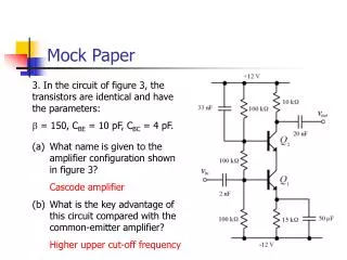
Mock Paper. 3. In the circuit of figure 3, the transistors are identical and have the parameters: b = 150, C BE = 10 pF, C BC = 4 pF. What name is given to the amplifier configuration shown in figure 3? Cascode amplifier

E N D
Mock Paper 3. In the circuit of figure 3, the transistors are identical and have the parameters: b = 150, CBE = 10 pF, CBC = 4 pF. • What name is given to the amplifier configuration shown in figure 3? • Cascode amplifier • What is the key advantage of this circuit compared with the common-emitter amplifier? • Higher upper cut-off frequency
(c) Calculate the quiescent base, emitter and collector voltages for the two transistors and the collector current of Q1. Quiescent assumptions: IB = 0, VBE = 0.5 V 24V dropped across three 100kW resistors, 8V across each: • = 150, CBE = 10 pF, CBC = 4 pF.
(d) Calculate the mid-band gain, the input impedance and the output impedance of the circuit. • = 150, CBE = 10 pF, CBC = 4 pF.
(e) Calculate the lower and upper cut-off frequencies of the amplifier for a source impedance of 1 kW. Lower cut-off • = 150, CBE = 10 pF, CBC = 4 pF.
(e) Calculate the lower and upper cut-off frequencies of the amplifier for a source impedance of 1 kW. Upper cut-off • = 150, CBE = 10 pF, CBC = 4 pF.
In the circuit shown in figure 4, assume that the forward biased diode voltage is 0.5 V. (f) Calculate the thermal noise voltage that appears across the resistor in terms of V/ÖHz T = 300 K k = 1.38×10⁻²³ J/K q = 1.6×10⁻¹⁹ C
(g) Calculate the additional noise voltage that appears across the resistor due to shot noise in the diode current (again in V/ÖHz). Hence calculate the total noise voltage across the resistor. T = 300 K k = 1.38×10⁻²³ J/K q = 1.6×10⁻¹⁹ C
4 The total maximum power dissipation of a class-B power amplifier is calculated to be 15 W. Given output transistors with a specification of TJmax = 150 °C, qJA = 40 °C/W, qJC = 1.5 °C/W: i. Calculate the power dissipated by each output transistor. ii. Calculate the minimum specifications for heatsinks that could be used for each transistor. iii. Calculate the minimum specification for a single heatsink that could be used by both transistors. Single heatsink must be twice the specification:
(b) In a common-emitter amplifier: • Explain why the base-collector capacitance of the transistor usually has the most influence over the upper cut-off frequency of the amplifier. • In a common-emitter amplifier, the base-collector capacitance is multiplied by the amplifier gain (plus one) due to the Miller effect. Consequently, it would usually appear to be an order of magnitude larger than the base-emitter capacitance • Suggest three ways in which the upper cut-off frequency of an amplifier can be increased. • Decrease the gain (reduces Miller effect) • Use a transistor with lower junction capacitances • Adopt a cascode configuration
(c) Explain, using supporting diagrams, how generalised impedance converter(s) can be used to simulate: i. A grounded inductance i.e. the circuit has the same input impedance as an inductance of CR2 Henries
(c) Explain, using supporting diagrams, how generalised impedance converter(s) can be used to simulate: ii. A floating inductance Again, the circuit has the same impedance as an inductance of CR2 Henries
(c) Explain, using supporting diagrams, how generalised impedance converter(s) can be used to simulate: iii. A frequency dependent negative resistance i.e. a frequency dependant negative resistance