Download
1 / 50
600 likes | 1.61k Vues
4 – Crystal Structure and Defects in Metals. Outline. Space Lattice & Unit Cell BCC FCC HCP Miller Indices Directions Planes Defects 0-D: solid solutions, vacancies 1-D: dislocations 2-D: Grain boundaries, twin boundaries. The Space Lattice and Unit Cells.

E N D
Outline • Space Lattice & Unit Cell • BCC • FCC • HCP • Miller Indices • Directions • Planes • Defects • 0-D: solid solutions, vacancies • 1-D: dislocations • 2-D: Grain boundaries, twin boundaries
The Space Lattice and Unit Cells • Atoms, arranged in repetitive 3-Dimensional pattern, in long range order (LRO) give rise to crystal structure. • Properties of solids depends upon crystal structure and bonding force. • An imaginary network of lines, with atoms at intersection of lines, representing the arrangement of atoms is called space lattice. Space Lattice • Unit cell is that block of • atoms which repeats itself • to form space lattice. • Materials arranged in short • range order are called • amorphous materials Unit Cell 3-2
Crystal Systems and Bravais Lattice • Only seven different types of unit cells are necessary to create all point lattices. • According to Bravais (1811-1863) fourteen standard unit cells can describe all possible lattice networks. • The four basic types of unit cells are • Simple • Body Centered • Face Centered • Base Centered 3-3
Types of Unit Cells • Cubic Unit Cell • a = b = c • α = β = γ = 900 • Tetragonal • a =b ≠ c • α = β = γ = 900 Body Centered Simple Face centered Body Centered Simple 3-4 After W.G. Moffatt, G.W. Pearsall, & J. Wulff, “The Structure and Properties of Materials,” vol. I: “Structure,” Wiley, 1964, p.47.)
Types of Unit Cells (Cont..) • Orthorhombic • a ≠ b ≠ c • α = β = γ = 900 • Rhombohedral • a =b = c • α = β = γ ≠ 900 Simple Base Centered Body Centered Face Centered Figure 3.2 Simple 3-5 After W.G. Moffatt, G.W. Pearsall, & J. Wulff, “The Structure and Properties of Materials,” vol. I: “Structure,” Wiley, 1964, p.47.)
Types of Unit Cells (Cont..) • Hexagonal • a ≠ b ≠ c • α = β = γ = 900 • Monoclinic • a ≠ b ≠ c • α = β = γ = 900 • Triclinic • a ≠ b ≠ c • α = β = γ = 900 Simple Base Centered Simple Figure 3.2 Simple 3-6 After W.G. Moffatt, G.W. Pearsall, & J. Wulff, “The Structure and Properties of Materials,” vol. I: “Structure,” Wiley, 1964, p.47.)
Principal Metallic Crystal Structures • 90% of the metals have either Body Centered Cubic (BCC), Face Centered Cubic (FCC) or Hexagonal Close Packed (HCP) crystal structure. • HCP is denser version of simple hexagonal crystal structure. FCC Structure HCP Structure BCC Structure 3-7
Body Centered Cubic (BCC) Crystal Structure • Represented as one atom at each corner of cube and one at the center of cube. • Each atom has 8 nearest neighbors. • Therefore, coordination number is 8. • Examples :- • Chromium (a=0.289 nm) • Iron (a=0.287 nm) • Sodium (a=0.429 nm) 3-8
BCC Crystal Structure (Cont..) • Each unit cell has eight 1/8 atom at corners and 1 full atom at the center. • Therefore each unit cell has • Atoms contact each other at cube diagonal (8x1/8 ) + 1 = 2 atoms Therefore, lattice constant a = 3-9
Atomic Packing Factor of BCC Structure Volume of atoms in unit cell Atomic Packing Factor = Volume of unit cell Vatoms = = 8.373R3 V unit cell = a3 = = 12.32 R3 8.723 R3 Therefore APF = = 0.68 12.32 R3 3-10
Face Centered Cubic (FCC) Crystal Structure • FCC structure is represented as one atom each at the corner of cube and at the center of each cube face. • Coordination number for FCC structure is 12 • Atomic Packing Factor is 0.74 • Examples :- • Aluminum (a = 0.405) • Gold (a = 0.408) 3-11
FCC Crystal Structure (Cont..) • Each unit cell has eight 1/8 atom at corners and six ½ atoms at the center of six faces. • Therefore each unit cell has • Atoms contact each other across cubic face diagonal (8 x 1/8)+ (6 x ½) = 4 atoms Therefore, lattice constant a = 3-12
Hexagonal Close-Packed Structure • The HCP structure is represented as an atom at each of 12 corners of a hexagonal prism, 2 atoms at top and bottom face and 3 atoms in between top and bottom face. • Atoms attain higher APF by attaining HCP structure than simple hexagonal structure. • The coordination number is 12, APF = 0.74. 3-13 After F.M. Miller, “Chemistry: Structure and Dynamics,” McGraw-Hill, 1984, p.296
HCP Crystal Structure (Cont..) • Each atom has six 1/6 atoms at each of top and bottom layer, two half atoms at top and bottom layer and 3 full atoms at the middle layer. • Therefore each HCP unit cell has • Examples:- • Zinc (a = 0.2665 nm, c/a = 1.85) • Cobalt (a = 0.2507 nm, c.a = 1.62) • Ideal c/a ratio is 1.633. (2 x 6 x 1/6) + (2 x ½) + 3 = 6 atoms 3-14 After F.M. Miller, “Chemistry: Structure and Dynamics,” McGraw-Hill, 1984, p.296
Atom Positions in Cubic Unit Cells • Cartesian coordinate system is use to locate atoms. • In a cubic unit cell • y axis is the direction to the right. • x axis is the direction coming out of the paper. • z axis is the direction towards top. • Negative directions are to the opposite of positive directions. • Atom positions are • located using unit • distances along the • axes. 3-15
Directions in Cubic Unit Cells • In cubic crystals, Direction Indices are vectorcomponents of directions resolved along each axes, resolved to smallest integers. • Direction indices are position coordinates of unit cell where the direction vector emerges from cell surface, converted to integers. 3-16
Procedure to Find Direction Indices Produce the direction vector till it emerges from surface of cubic cell z (1,1/2,1) - (0,0,0) = (1,1/2,1) (1,1/2,1) Determine the coordinates of point of emergence and origin y 2 x (1,1/2,1) = (2,1,2) (0,0,0) Subtract coordinates of point of Emergence by that of origin x The direction indices are [212] NO Convert them to smallestpossible integer by multiplying by an integer. All are integers? YES Are any of the direction vectors negative? NO YES Represent the indices in a square bracket without comas with a over negative index (Eg: [121]) Represent the indices in a square bracket without comas (Eg: [212] ) 3-17
Direction Indices - Example • Determine direction indices of the given vector. Origin coordinates are (3/4 , 0 , 1/4). Emergence coordinates are (1/4, 1/2, 1/2). Subtracting origin coordinates from emergence coordinates, (1/4, 1/2, 1/2)-(3/4 , 0 , 1/4) = (-1/2, 1/2, 1/4) Multiply by 4 to convert all fractions to integers 4 x (-1/2, 1/2, 1/4) = (-2, 2, 1) Therefore, the direction indices are [ 2 2 1 ] 3-18
Miller Indices • Miller Indices are are used to refer to specific lattice planes of atoms. • They are reciprocals of the fractional intercepts (with fractions cleared) that the plane makes with the crystallographic x,y and z axes of three nonparallel edges of the cubic unit cell. z Miller Indices =(111) y x 3-19
Miller Indices - Procedure Choose a plane that does not pass through origin Determine the x,y and z intercepts of the plane Find the reciprocals of the intercepts Clear fractions by multiplying by an integer to determine smallest set of whole numbers Fractions? Place a ‘bar’ over the Negative indices Enclose in parenthesis (hkl)where h,k,l are miller indicesof cubic crystal plane forx,y and z axes. Eg: (111) 3-20
Intercepts of the plane at x,y & z axes are 1, ∞ and ∞ Taking reciprocals we get (1,0,0). Miller indices are (100). ******************* Intercepts are 1/3, 2/3 & 1. taking reciprocals we get (3, 3/2, 1). Multiplying by 2 to clear fractions, we get (6,3,2). Miller indices are (632). Miller Indices - Examples z (100) y x x 3-21
Plot the plane (101) Taking reciprocals of the indices we get (1 ∞ 1). The intercepts of the plane are x=1, y= ∞ (parallel to y) and z=1. ****************************** Plot the plane (2 2 1) Taking reciprocals of the indices we get (1/2 1/2 1). The intercepts of the plane are x=1/2, y= 1/2 and z=1. Miller Indices - Examples Figure EP3.7 a 3-22
Miller Indices - Example • Plot the plane (110) The reciprocals are (1,-1, ∞) The intercepts are x=1, y=-1 and z= ∞ (parallel to z axis) To show this plane a single unit cell, the origin is moved along the positive direction of y axis by 1 unit. z (110) y x 3-23
Miller Indices – Important Relationship • Direction indices of a direction perpendicular to a crystal plane are same as miller indices of the plane. • Example:- • Interplanar spacing between parallel closest planes with same miller indices is given by z y (110) [110] x 3-24
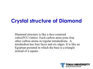
Comparison of FCC and HCP crystals • Both FCC and HCP are close packed and have APF 0.74. • FCC crystal is close packed in (111) plane while HCP is close packed in (0001) plane. 3-28 After W.G. Moffatt, G.W. Pearsall, & J. Wulff, “The Structure and Properties of Materials,” vol. I: “Structure,” Wiley, 1964, p.51.)
Structural Difference between HCP and FCC Plane A Consider a layer of atoms (Plane ‘A’) ‘a’ void ‘b’ void Another layer (plane ‘B’) of atoms is placed in ‘a’ Void of plane ‘A’ Plane A Plane B ‘a’ void ‘b’ void Third layer of Atoms placed in ‘b’ Voids of plane ‘B’. (Identical to plane ‘A’.) HCP crystal. Third layer of Atoms placed in ‘a’ voids of plane ‘B’. Resulting In 3rd Plane C. FCC crystal. Plane A Plane A Plane B Plane B Plane A Plane C Figure 3.20 3-29
Volume Density Mass/Unit cell • Volume density of metal = • Example:- Copper (FCC) has atomic mass of 63.54 g/mol and atomic radius of 0.1278 nm. = Volume/Unit cell a= = = 0.361 nm Volume of unit cell = V= a3 = (0.361nm)3 = 4.7 x 10⁻²⁹ m3 FCC unit cell has 4 atoms. Mass of unit cell = m = = 4.22 x 10⁻²⁸ Mg 3-30
Metallic Solid Solutions • Alloys are used in most engineering applications. • An Alloy is a mixture of two or more metals and nonmetals. • Example: • Cartridge brass is binary alloy of 70% Cu and 30% Zinc. • Inconel is a nickel based superalloy with about 10 elements. • Solid solution is a simple type of alloy in which elements are dispersed in a single phase. 4-14
Substitutional Solid Solution • Solute atoms substitute for parent solvent atom in a crystal lattice. • The structure remains unchanged. • Lattice might get slightly distorted due to change in diameter of the atoms. • Solute percentage in solvent can vary from fraction of a percentage to 100% Solvent atoms Figure 4.14 Solute atoms 4-15
Substitutional Solid Solution (Cont..) • The solubility of solids is greater if • The diameter of atoms does not differ by more than 15% • Crystal structures are similar. • Not much difference in electronegativity (or compounds will be formed). • Have same valence. • Examples:- 4-16
Interstitial Solid Solution • Solute atoms fit in between the voids (interstices) of solvent atoms. • Solvent atoms in this case should be much larger than solute atoms. • Example:- between 912 and 13940C, interstitial solid solution of carbon in γ iron (FCC) is formed. • A maximum of 2.8% of carbon can dissolve interstitially in iron. Iron atoms r00.129nm Carbon atoms r=0.075nm 4-17
Crystalline Imperfections • No crystal is perfect. • Imperfections affect mechanical properties, chemical properties and electrical properties. • Imperfections can be classified as • Zero dimensional point defects. • One dimensional / line defects (dislocations). • Two dimensional defects. • Three dimensional defects (cracks). 4-18
Point Defects – Vacancy • Vacancy is formed due to a missing atom. • Vacancy is formed (one in 10000 atoms) during crystallization or mobility of atoms. • Energy of formation is 1 eV. • Mobility of vacancy results in cluster of vacancies. • Also caused due to plastic defor- -mation, rapid cooling or particle bombardment. Figure: Vacancies moving to form vacancy cluster 4-19
Point Defects - Interstitially • Atom in a crystal, sometimes, occupies interstitial site. • This does not occur naturally. • Can be induced by irradiation. • This defects caused structural distortion. Figure 4.16b 4-20
Point Defects in Ionic Crystals • Complex as electric neutrality has to be maintained. • If two oppositely charged particles are missing, cation-anion di-vacancy is created. This is Scohttky defect. • Frenkel defect is created when cation moves to interstitial site. • Impurity atoms are also considered as point defects. 4-21
Yield Stress in Crystalline Materials t Initial Position t t Saddle Point t For Mg Single Crystal predicts a yield stress of 17.2*0.5=8.6GPa Measured yield stress is 0.7MPa 10,000 times less than expected! At Saddle Point
Line Defects – (Dislocations) • Discrepancy is due to dislocations. • Dislocations are lattice distortions centered around a line. • Formed during • Solidification • Permanent Deformation • Vacancy condensation • Different types of line defects are • Edge dislocation • Screw dislocation • Mixed dislocation 4-22
Edge Dislocation • Created by insertion of extra half planes of atoms. • Positive edge dislocation • Negative edge dislocation • Burgers vector Shows displa- cement of atoms (slip). Burgers vector 4-23 After M. Eisenstadt, “Introduction to Mechanical Properties of Materials,” Macmillan, 1971, p.117 After A.G. Guy , “Essentials of Materials Science,” McGraw-Hill, 1976, p.153
Screw Dislocation • Created due to shear stresses applied to regions of a perfect crystal separated by cutting plane. • Distortion of lattice in form of a spiral ramp. • Burgers vector is parallel to dislocation line. 4-24 After M. Eisenstadt, “Introduction to Mechanical Properties of Materials,” Macmillan, 1971, p.118
Mixed Dislocation • Most crystal have components of both edge and screw dislocation. • Dislocation, since have irregular atomic arrangement will appear as dark lines when observed in electron microscope. Dislocation structure of iron deformed 14% at –1950C (After John Wolff et al., “Structure and Properties of Materials,” vol 3: “Mechanical Properties,” Wiley, 1965, p.65. (After “Metals Handbook” vol. 8, 8th ed., American Society of Metals, 1973, p.164)
Electron produced by heated tungsten filament. Accelerated by high voltage (75 - 120 KV) Electron beam passes through very thin specimen. Difference in atomic arrangement change directions of electrons. Beam is enlarged and focused on fluorescent screen. Transmission Electron Microscope Collagen Fibrils of ligament as seen in TEM (After L.E. Murr, “ Electron and Ion Microscopy and Microanalysis, “ Marcel Decker, 1982, p.105)
TEM (..Cont) • TEM needs complex sample preparation • Very thin specimen needed ( several hundred nanometers) • High resolution TEM (HRTEM) allows resolution of 0.1 nm. • 2-D projections of a crystal with accompanying defects can be observed. Low angle boundary As seen In HTREM
Electron source generates electrons. Electrons hit the surface and secondary electrons are produced. The secondary electrons are collected to produce the signal. The signal is used to produce the image. The Scanning Electron Microscope Figure 4.31 SEM of fractured metal end After V.A. Phillips, “Modern Photographic techniques and Their Applications,” Wiley, 1971, p.425
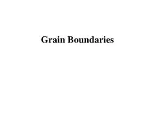
Grain Boundaries • Grain boundaries separate grains. • Formed due to simultaneously growing crystals meeting each other. • Width = 2-5 atomic diameters. • Some atoms in grain boundaries have higher energy. • Restrict plastic flow and prevent dislocation movement. 3D view of grains Grain Boundaries In 1018 steel 4-27 (After A.G. Guy, “ Essentials of materials Science,” McGraw-Hill, 1976.)
Planar Defects • Grain boundaries, twins, low/high angle boundaries, twists and stacking faults • Free surface is also a defect : Bonded to atoms on only one side and hence has higher state of energy Highly reactive • Nanomaterials have small clusters of atoms and hence are highly reactive.
Twin Boundaries • Twin: A region in which mirror image pf structure exists across a boundary. • Formed during plastic deformation and recrystallization. • Strengthens the metal. Twin Plane Twin
Observing Grain Boundaries - Metallography • To observe grain boundaries, the metal sample must be first mounted for easy handling • Then the sample should be ground and polished with different grades of abrasive paper and abrasive solution. • The surface is then etched chemically. • Tiny groves are produced at grain boundaries. • Groves do not intensely reflect light. Hence observed by optical microscope. 4-28 After M. Eisenstadt, “Introduction to Mechanical Properties of Materials,” Macmillan, 1971, p.126
Grain Size • Affects the mechanical properties of the material • The smaller the grain size, more are the grain boundaries. • More grain boundaries means higher resistance to slip (plastic deformation occurs due to slip). • More grains means more uniform the mechanical properties are. 4-30
Measuring Grain Size • ASTM grain size number ‘n’ is a measure of grain size. N = 2 n-1 N = Number of grains per square inch of a polished and etched specimen at 100 x. n = ASTM grain size number. N < 3 – Coarse grained 4 < n < 6 – Medium grained 7 < n < 9 – Fine grained N > 10 – ultrafine grained 200 X 200 X 1018 cold rolled steel, n=10 1045 cold rolled steel, n=8 4-31