Download
1 / 19
250 likes | 637 Vues
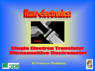
Nano-electronics:. 500 nm. Single Electron Transistor Ultrasensitive Electrometer. By Francesco Maddalena. 1. Introduction. To uphold Moore’s Law in the future a new generation of devices that fully operate in the “ quantum realm” is needed: NANODEVICES.

E N D
Nano-electronics: 500 nm Single Electron Transistor Ultrasensitive Electrometer By Francesco Maddalena
1. Introduction To uphold Moore’s Law in the future a new generation of devices that fully operate in the “quantum realm” is needed: NANODEVICES One of the most interesting types of nanodevices is the Single-Electron Transistor The Single-Electron Transistor can perform the same functions as a common transistor yet it will probably not replace the nowadays FETs Instead it can be used as ultra-sensitive electrometer
2. Principles of the SET The simplest of the single-electron tunneling devices is the single-electron box (SEB) Electrons can tunnel though the junction from the source to the island putting excess electrons on it By changing the gate voltage one can add or subtract single electrons from the island The number of excess electrons depend on the electrostatic energy of the SEB:
2. Principles of the SET The energy of the SEB varies quadratcally with QG at the degeneracy points tunneling will occur The charge Q on the island will depend on the voltage Vgand it will increase discretely at T=0 (blue line) At finite temperatures the Q/Vg dependence will be smoothed or even disappear
2. Principles of the SET The single-electron transistor (SET) is an expansion of the SEB The SET has a drain, a source and a gate electrode (as a normal FET) and a island contained between two tunneling junctions The current flow between the drain and the source and the charge on the island is regulated by the gate voltage VG via the Coulomb Blockade
2. Principles of the SET Drain The SET is a relative simple device to build The the SET can be constructed by using Electron-beam lithography (EBL) and evaporations techniques such as evaporation at different deposition angles Source Island Gate 500 nm
2. Principles of the SET Similarly to the single electron box the island of the SET can be charged by excess electrons on it If adding an extra excess electron on the island (by tunneling) causes the energy to increase the system will be then energetically forbidden This represents a barrier for adding excess electrons and is defined as the Coulomb blockade
2. Principles of the SET The SET allows a current between the drain and source electrodes if the value of the drain-source voltage is higher than a critical threshold voltage VT If there are no excess electrons on the island and the gate voltage is zero then the threshold voltage is equal to: By changing the gate voltage we can lower the threshold voltage since the energy of the system depends on the gate charge The gate voltage for which the threshold voltage is zero is equal to:
2. Principles of the SET We can plot the I/V characteristics of the SET: We can also plot the value of the threshold voltage against the value of the gate voltage This is called the Stability Diagram of the SET
2. Principles of the SET • The performance of the SET is altered by external parameters: • At finite temperatures the Coulomb blockade of the SET is thermally whashed out. • For a good performance the charging energy of the SET must be much higher than the thermal energy • Most SETs work properly only at temperatures close to liquid Helium temperatures, however room temperature SETs have been made • External charges influence the SET, shifting the threshold voltage, and can be seen as an extra gate charge
3. Charge Sensitivity The SET has many applications: it can function as a regular transistor, memory storage device and has great potential in metrology as ultra-sensitive electrometer with an high charge sensitivity The SET can be seen as a linear amplifier The charge sensitivity for an amplifier is defined as: Where SV(w) is the spectral density of the voltage noise, Zin the input impedance and w the frequency
3. Charge Sensitivity • Charge sensitivity is limited by different types of noise: • Thermal Noise: Johnson-Nyquist noise depended on the impendance and temperature of the system • Shot Noise: generated by random tunneling of electrons across the island junctions • Flicker Noise (a.k.a. Pink Noise or 1/f-noise): still an ill-understood process with different possible causes • For the SET the Flicker noise is originated principally from: 1-Mobility fluctuations in conductors 2- Charge fluctuations at the surface in contact with the oxide layer in semiconductors
3. Charge Sensitivity The SET can be used as charge meter either in DC or RF mode In the DC mode the current or the conductance are measured Maximum sensitivity is achieved by setting VG such that the current is at half maximum
3. Charge Sensitivity In the RF mode the measured value is usually the damping of an high-frequency resonant circuit The RF mode has the advantage to eliminate 1/f noise at high frequencies The resonant circuit and the SET can be physically separated permitting the SET to be independently cooled at low temperatures (EC>>kT)
3. Charge Sensitivity If we operate the SET at low temperatures the Johnson-Nyquist noise due to thermal effects will be negligible We can also reduce the Flicker noise (proportional to 1/f) to negligible values if we operate the SET in the rf-domain Operating the SET at high frequencies ( ) will reduce the Flicker noise to values that can be ignored and at low frequencies ( ) a feedback can compensate for the noise Under the above mentioned conditions the only significant noise source is the Shot-noise caused by the random tunneling
3. Charge Sensitivity With the shot noise as significant noise source the spectral density of the voltage noise SV is given by the Fourier transform of the auto-correlation function of the voltage noise: Coulomb blockade parameter From SV we can then write an expression for the charge sensitivity:
3. Charge Sensitivity For optimal parameters: (neglects co-tunneling processes) and low temperatures (EC>> kT): a factor 10 higher than the theoretical limit Experimentally determined values of d Q are low as can be reached, a factor 10 higher than the (theoretical) optimal value FET theoretical optimal limit: The SET is a factor 1000 better than the FET!
4. Conclusions The Single-electron transistor is capable of controlling the movement of single elementary charges Technologically it is quite easy to build It has various applications, some of them equal to the ‘classical’ transistors used nowadays but will probably be the replacement of the Field-effect transistor It has an high charge sensitivity, a factor 1000 better than the FET and it is a very good candidate for ultra-sensitive charge measurements
5. References Devoret M.H. and Schoelkopf R.J.- Nature (2000), vol 406, p.1039 Schoelkopf et. al.- Science (1998), 280 (5367), p1238 Zimmerli et. al.- Appl. Phys. Lett. (1992), 61 (2), p237