Download
1 / 24
471 likes | 1.16k Vues
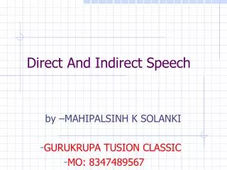
Chapter 3. Carrier Action. P honon. P hoton. P hoton. Direct and Indirect Semiconductors. E - k Diagrams. E c. E c. E v. E v. GaAs, GaN (direct semiconductors). Si, Ge (indirect semiconductors). Large change in momentum is required for recombination

E N D
Chapter 3 Carrier Action Phonon Photon Photon Direct and Indirect Semiconductors E-k Diagrams Ec Ec Ev Ev GaAs, GaN (direct semiconductors) Si, Ge (indirect semiconductors) • Large change in momentum is required for recombination • Momentum is conserved by mainly phonon (vibration) emission + photon emission • Little change in momentumis required for recombination • Momentum is conserved by photon (light) emission
Chapter 3 Carrier Action Values under arbitrary conditions Deviation from equilibrium values Equilibrium values Excess Carrier Concentrations • Positive deviation corresponds to a carrier excess, while negative deviation corresponds to a carrier deficit. • Charge neutrality condition:
Chapter 3 Carrier Action “Low-Level Injection” • Often, the disturbance from equilibrium is small, such that the majoritycarrier concentration is not affected significantly: • For an n-type material • For a p-type material • Low-level injection condition • However, the minority carrier concentration can be significantly affected.
Chapter 3 Carrier Action Indirect Recombination Rate • Suppose excess carriers are introduced into an n-typeSi sample by shining light onto it. At time t = 0, the light is turned off. How does p vary with time t > 0? • Consider the rate of hole recombination: NT : number of R–G centers/cm3 Cp : hole capture coefficient • In the midst of relaxing back to the equilibrium condition, the holegeneration rate is small and is taken to be approximately equal to its equilibrium value:
Chapter 3 Carrier Action Indirect Recombination Rate • The net rate of change in p is therefore: where • For holes in n-type material • Similarly, where • For electrons in p-type material
Chapter 3 Carrier Action Minority Carrier Lifetime • The minority carrier lifetimeτis the average time for excess minority carriers to “survive” in a sea of majority carriers. • The value of τ ranges from 1 ns to 1 ms in Si anddepends on the density ofmetallic impurities and the density of crystalline defects. • Thedeep trapsoriginated from impurity and defects capture electrons or holes to facilitate recombination and are calledrecombination-generation centers.
Chapter 3 Carrier Action Photoconductor • Photoconductivity is an optical and electrical phenomenon in which a material becomes more electrically conductive due to the absorption of electro-magnetic radiation such as visible light, ultraviolet light, infrared light, or gamma radiation. • When light is absorbed by a material like semiconductor, the number of free electrons and holes changes and raises the electrical conductivity of the semiconductor. • To cause excitation, the light that strikes the semiconductor must have enough energy to raise electrons across the band gap.
Chapter 3 Carrier Action Example: Photoconductor • Consider a sample of Si at 300 K doped with 1016 cm–3 Boron, with recombination lifetime 1 μs. It is exposed continuously to light, such that electron-hole pairs are generated throughout the sample at the rate of 1020 per cm3 per second, i.e. the generation rate GL = 1020/cm3/s. • a) What are p0 and n0? • b) What are Δn and Δp? • Hint: In steady-state, generation rate equals recombination rate
Chapter 3 Carrier Action Example: Photoconductor • Consider a sample of Si at 300 K doped with 1016 cm–3 Boron, with recombination lifetime 1 μs. It is exposed continuously to light, such that electron-hole pairs are generated throughout the sample at the rate of 1020 per cm3 per second, i.e. the generation rate GL = 1020/cm3/s. • c) What are p and n? • d) What are np product? • Note: The np product can be very different from ni2 in case of perturbed/agitated semiconductor
Chapter 3 Carrier Action Net Recombination Rate (General Case) • For arbitrary injection levels and both carrier types in a non-degenerate semiconductor, the net rate of carrier recombination is: where • ET : energy level of R–G center
Chapter 3 Carrier Action Area A, volume A.dx JN(x) JN(x+dx) dx Continuity Equation • Consider carrier-flux into / out of an infinitesimal volume: Flow of current Flow of electron
Chapter 3 Carrier Action Continuity Equation • Taylor’s Series Expansion • The Continuity Equations
Chapter 3 Carrier Action Minority Carrier Diffusion Equation • The minority carrier diffusion equations are derived from the general continuity equations, and are applicable only for minority carriers. • Simplifying assumptions: • The electric field is small, such that: • For p-type material • For n-type material • Equilibrium minority carrier concentration n0 and p0 are independent of x (uniform doping). • Low-level injection conditions prevail.
Chapter 3 Carrier Action Minority Carrier Diffusion Equation • Starting with the continuity equation for electrons: • Therefore • Similarly
Chapter 3 Carrier Action Carrier Concentration Notation • The subscript “n” or “p” is now used to explicitly denote n-type or p-type material. • pn is the hole concentration in n-type material • np is the electron concentration in p-type material • Thus, the minority carrier diffusion equations are:
Chapter 3 Carrier Action Simplifications (Special Cases) • Steady state: • No diffusion current: • No thermal R–G: • No other processes:
Chapter 3 Carrier Action Minority Carrier Diffusion Length • Consider the special case: • Constant minority-carrier (hole) injection at x = 0 • Steady state, no light absorption for x > 0 • The hole diffusion length LP is defined to be: Similarly,
Chapter 3 Carrier Action Minority Carrier Diffusion Length • The general solution to the equation is: • A and B are constants determined by boundary conditions: • Therefore, the solution is: • Physically, LP and LN represent the average distance that a minority carrier can diffuse before it recombines with majority a carrier.
Chapter 3 Carrier Action Example: Minority Carrier Diffusion Length • Given ND=1016 cm–3, τp = 10–6 s. Calculate LP. • From the plot,
Chapter 3 Carrier Action Quasi-Fermi Levels • Whenever Δn =Δp ≠0then np ≠ ni2 and we are at non-equilibrium conditions. • In this situation, now we would like to preserve and use the relations: • On the other hand, both equations imply np = ni2, which does not apply anymore. • The solution is to introduce to quasi-Fermi levels FN and FP such that: • The quasi-Fermi levels is useful to describe the carrier concentrations under non-equilibrium conditions
Chapter 3 Carrier Action Example: Quasi-Fermi Levels • Consider a Si sample at 300 K with ND = 1017 cm–3 and Δn = Δp = 1014 cm–3. • The sample is an n-type • a) What are p and n? • b) What is the np product?
Chapter 3 Carrier Action Example: Quasi-Fermi Levels • Consider a Si sample at 300 K with ND = 1017 cm–3 and Δn = Δp = 1014 cm–3. 0.417 eV Ec FN • c) Find FN and FP? Ei FP Ev 0.238 eV
Chapter 2 Carrier Action Homework 3 • 1. (6.17) • A semiconductor has the following properties:DN = 25 cm2/s τn0 = 10–6 s • DP = 10 cm2/s τp0 = 10–7 s • The semiconductor is a homogeneous, p-type (NA = 1017 cm–3) material in thermal equilibrium for t ≤ 0. At t = 0, an external source is turned on which produces excess carriers uniformly at the rate GL = 1020 cm–3 s–1. At t = 2×10⁻⁶ s, the external source is turned off. (a) Derive the expression for the excess-electron concentration as a function of time for 0 ≤ t ≤ ∞ (b) Determine the value of the excess-electron concentration at (i) t = 0, (ii) t = 2×10⁻⁶ s, and (iii) t = ∞ (c) Plot the excess electron concentration as a function of time. • 2. (4.38) • Problem 3.24Pierret’s “Semiconductor Device Fundamentals”. • Deadline: 10 May 2012, at 08:00.